As consumer electronics evolve toward higher performance and smaller form factors, the demand for HDI PCB (High-Density Interconnect Printed Circuit Board) technology continues to escalate. From smartphones and tablets to wearable devices and high-speed communication modules, HDI PCB fabrication has become a core enabling technology for achieving ultra-compact, lightweight, and highly functional electronic products.
Among global HDI PCB manufacturers, SprintPCB PCB solutions stand out for their advanced fabrication capabilities, including microvias, buried vias, blind vias, and ultra-fine circuit processing. Their HDI PCB solutions support 4–60 layers, high-performance materials, ultra-thin board constructions, and precision technologies designed for next-generation electronic innovations.

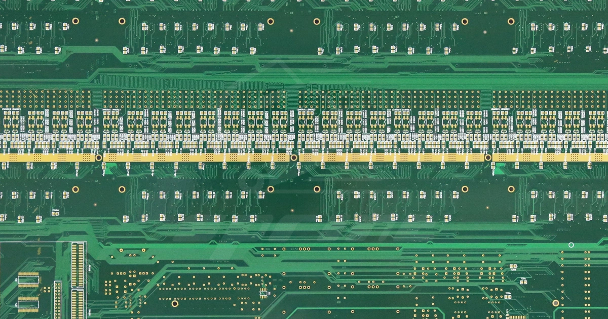
An HDI PCB (High-Density Interconnect Printed Circuit Board) is a type of circuit board designed with ultra-fine traces, microvias, and compact multilayer structures to achieve high wiring density in limited space. Unlike standard PCBs, an HDI PCB uses blind vias, buried vias, and via-in-pad technology to shorten signal paths, improve electrical performance, and support dense component placement. This advanced design enables better signal integrity, reduced board thickness, and higher functional integration, making HDI PCB technology essential for modern devices such as smartphones, tablets, wearables, and high-speed communication modules.
The structural design and manufacturing technologies behind an HDI PCB are what give it superior density, electrical performance, and long-term reliability. Compared with traditional multilayer boards, an HDI PCB integrates micro-scale interconnect technologies, ultra-fine routing capabilities, and advanced lamination processes that allow engineers to achieve compact system designs without sacrificing signal quality.
One of the most defining features of an HDI PCB is the extensive use of microvias. These tiny, laser-drilled vias—often blind or buried—enable extremely short interconnect distances between layers. Because microvias have significantly lower parasitic capacitance and inductance than traditional mechanical vias, they help maintain excellent signal fidelity, especially in high-speed and RF systems.
Microvias in an HDI PCB provide several key advantages:
Increased routing channels in dense component areas
Enhanced electrical performance with reduced signal distortion
Greater flexibility when designing under fine-pitch BGAs and CSPs
Reliable mechanical structure with lower via aspect ratios
For modern devices requiring compact layouts and high-speed data transmission, microvias are a technical necessity.
Fine-line circuitry is another pillar of HDI PCB design. As chip footprints shrink and component pitches become tighter, routing signals within constrained areas requires exceptional manufacturing precision.
With trace/space capabilities as small as 0.075 mm, HDI PCBs allow designers to:
Route high-density signals between ultra-fine BGA pad
Reduce the overall board size without sacrificing functionality
Improve signal path efficiency by minimizing unnecessary detours
Such fine routing is particularly important in consumer electronics like smartphones, tablets, and wearable devices, where engineers rely on HDI PCB technology to maintain compact yet powerful designs.
To achieve complex interconnect architectures, an HDI PCB often uses sequential lamination—a process in which multiple build-up layers are added step by step. This technique supports advanced HDI structures such as:
3+N+3 stack-ups
4+N+4 designs
Any-layer interconnect HDI (where every layer can connect freely)
Sequential lamination enables the integration of stacked or staggered microvias, providing both mechanical strength and routing flexibility. This is essential for high-performance applications where electrical and thermal reliability must be maintained even under compact conditions.
Specialized via technologies also contribute to the structural sophistication of the HDI PCB.
Via-in-pad structures place microvias directly beneath component pads, enabling:
Shorter signal paths
Cleaner high-speed transitions
Better thermal dissipation
More efficient use of board space
For circuits that require extremely low noise and minimal stub effects, back-drilled vias are used to eliminate unused via barrels, further improving signal integrity at high frequencies.
Filled and capped vias also ensure that HDI PCB surfaces remain flat, which is especially important for components with sensitive soldering requirements such as micro-BGAs.
Because an HDI PCB contains numerous microvias and ultra-thin dielectrics, maintaining precise registration between layers is crucial. Advanced optical alignment systems and automated inspection technologies ensure that:
Layer-to-layer alignment remains consistent
Microvias land accurately on inner-layer pads
Signal integrity is not compromised due to misalignment
This high level of precision is one of the reasons why HDI PCB solutions are relied upon for mission-critical electronics, where even small deviations can lead to performance degradation.
To complement the structural features above, HDI PCB manufacturing also incorporates advanced materials and surface treatments. High-performance FR4, halogen-free laminates, and Rogers materials are frequently used to achieve:
Stable dielectric performance
Enhanced thermal reliability
Reduced signal loss in high-frequency environments
Surface finishes such as ENIG, immersion silver, and electrolytic gold ensure excellent solderability and long-term oxidation resistance—an essential requirement for densely packed HDI PCB assemblies.
HDI PCB technology has become fundamental to modern electronics, enabling compact, high-performance, and reliable designs across industries such as mobile devices, automotive electronics, medical equipment, and high-speed communication systems. Through advanced fabrication techniques including micro blind and buried vias, ultra-fine line processing, and sequential lamination, HDI PCB allows engineers to achieve higher functionality in smaller spaces with superior signal integrity.
SprintPCB HDI PCB solutions offer best-in-class manufacturing capabilities, including up to 60 layers, microvia drilling down to 0.075mm, fine line etching at 0.075mm, and a wide range of materials and finishes. Their experience, precision manufacturing, and comprehensive engineering support make SprintPCB an excellent partner for any company seeking high-density, high-reliability PCB solutions.

Customer support