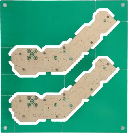
 Copper on both sides supporting SMD and through-hole components
High cost-effectiveness with flexible layout options
Typical for power modules and consumer electronics
Allows for higher circuit density than single-sided designs
Ideal balance between performance and production cost for mid-range applications
| Feature | Technical specification |
| Number of layers | 2 Layers |
| Materials | FR-4 standard, FR-4 high performance, FR-4 halogen-free |
| Copper weights (finished) | 0.5 oz – 6 oz |
| PCB Thickness | 0.40 mm – 6.0 mm |
| Max. dimensions | 620 mm x 720 mm |
| Min. track and gap | 0.075 mm / 0.075 mm |
| Min. mechanical drill | 0.15 mm |
| Surface finishes available | HASL (SnPb), LF HASL (SnNiCu), OSP, ENIG, Immersion Tin, Immersion Silver, Electrolytic gold, Gold fingers |

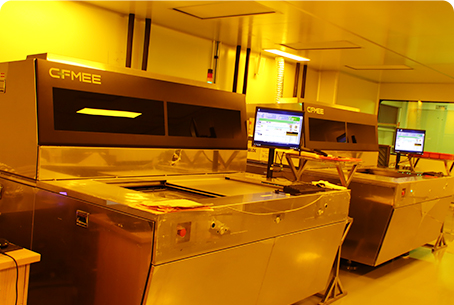
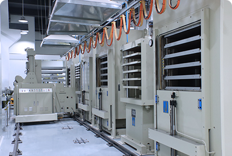
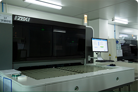
Engineering Support

Prototyping Services

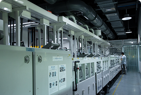
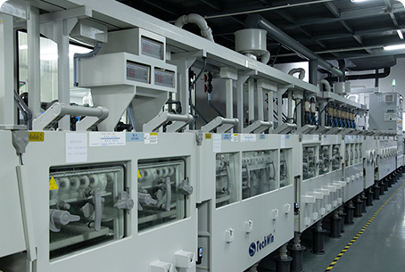
Fast Turnaround

Seamless Transition to Mass Production
 How does the trace routing differ in double sided PCBs compared to single sided PCBs? What are the advantages of double sided PCBs? What is the process of manufacturing double sided PCBs? What is a double sided PCB?
Customer support