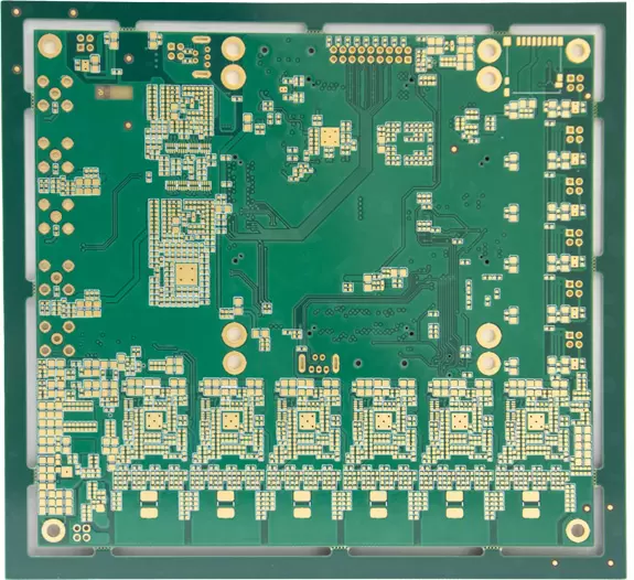
Micro-blind and buried vias for ultra-fine circuitry
Maximizes space savings and functional density
Enables better signal integrity with shorter interconnections
Supports higher layer counts in thinner, lighter board structures
Used in smartphones, tablets and wearable electronics
| Feature | Technical specification |
| Number of layers | 4 – 60 layers |
| HDI Builds | 3+N+3, 4+N+4, any layer in R&D |
| PCB thickness | 0.40 mm – 6.0 mm |
| Copper weights (finished) | 0.5 OZ – 6 OZ |
| Materials | High performance FR4, halogen-free FR4, Rogers |
| Max. dimensions | 620 mm x 720 mm |
| Min. track and gap | 0.075 mm / 0.075 mm |
| Min. mechanical drill | 0.15 mm |
| Surface finishes available | HASL (SnPb), LF HASL (SnNiCu), OSP, ENIG, Immersion Tin, Immersion Silver, Electrolytic gold, Gold fingers |
| Minimun laser drill | 0.10mm standard, 0.075mm advance |
| Special Processes | Blind/Buried Vias, Via-in-pad, Backdrill, Sideplating,Countersunk Holes |

Engineering Support

Prototyping Services

Fast Turnaround

Seamless Transition to Mass Production
 How do I select materials for HDI? Why should I turn to HDI PCBs? What is the laser drill accuracy? How does HDI PCBs keep my cost down? What is a HDI PCB? Are HDI PCBs more expensive than standard PCBs?
 Yes, HDI PCBs usually cost more due to complex manufacturing processes, but the benefits in performance and size often justify the higher price.

Customer support