 4-60 layers for ultra-high routing density
Excellent signal integrity and electromagnetic compatibility
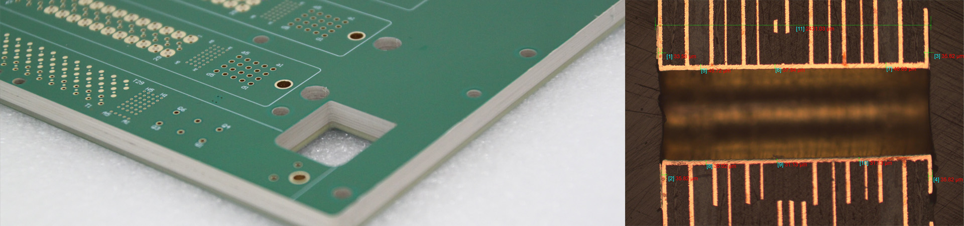
Support for blind & buried vias, via-in-pad, and impedance control
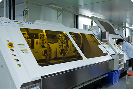
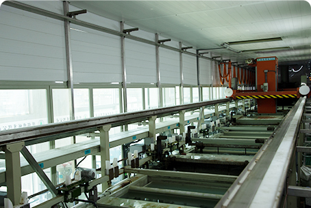
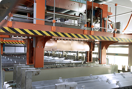
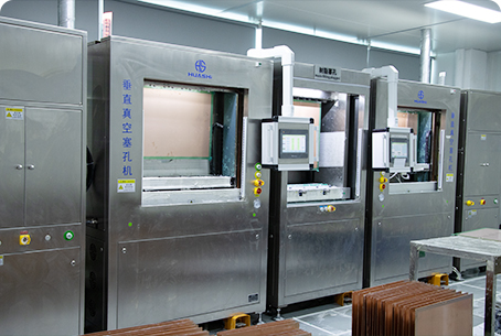
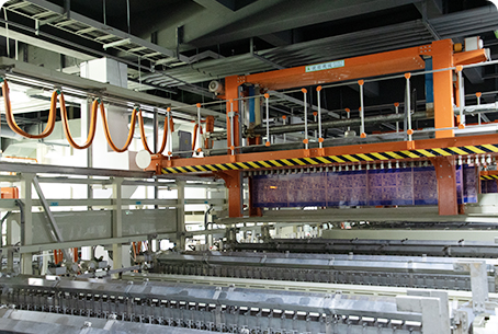
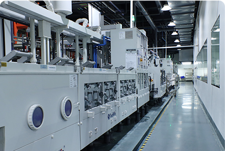
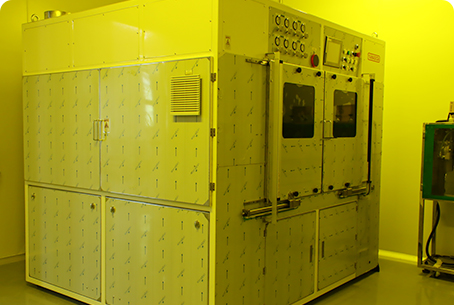
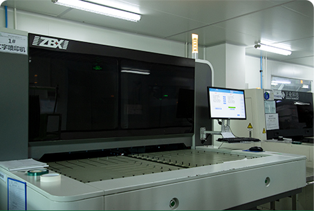
Engineered and manufactured with precision at SprintPCB's advanced facility
Used in servers, networking equipment and high-end medical devices
At SprintPCB, we specialize in designing and manufacturing multilayer PCBs that meet the highest standards of quality and performance. With up to 60 layers, our PCBs are built for ultra-high routing density, making them ideal for complex and compact electronic devices. Whether you're working on cutting-edge servers, networking equipment, or high-end medical devices, SprintPCB provides reliable solutions that ensure exceptional signal integrity and electromagnetic compatibility (EMC).
Up to 60 Layers for Ultra-High Routing Density
Our multilayer PCBs support up to 60 layers, enabling high-density routing for the most complex circuits. This makes them perfect for high-performance applications where space is limited but reliability is critical.
Superior Signal Integrity & Electromagnetic Compatibility (EMC)
Designed with advanced manufacturing techniques, our multilayer PCBs maintain excellent signal integrity even in high-frequency applications. We ensure superior EMC performance, reducing electromagnetic interference (EMI) for reliable operation.
Support for Blind & Buried Vias, Via-in-Pad, and Impedance Control
SprintPCB’s multilayer PCBs can accommodate advanced features such as blind and buried vias, via-in-pad designs, and precise impedance control. These options allow for enhanced design flexibility and are essential for high-speed digital and analog signal processing.
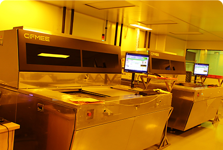
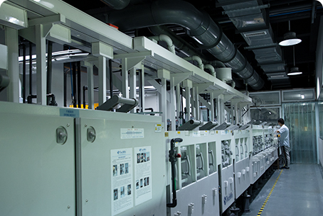
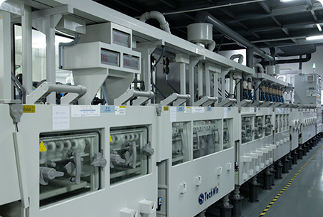
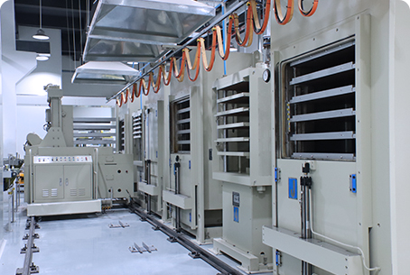
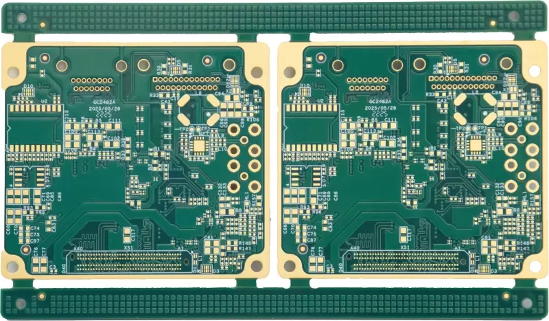
Precision Engineering & Manufacturing
All of our multilayer PCBs are engineered and manufactured with precision at SprintPCB's state-of-the-art facility. Our rigorous quality control processes ensure that every board meets the highest standards for performance, durability, and reliability.
Versatile Applications
SprintPCB’s multilayer PCBs are used in a wide range of industries, including server infrastructure, networking equipment, and medical devices. Our solutions are designed to handle the most demanding environments while delivering unmatched performance and longevity.
| Feature | Technical specification |
|---|---|
| Number of layers | 4 – 60 layers |
| PCB thickness | 0.40 mm – 7.0 mm |
| Copper weights (finished) | 0.5 OZ – 6 OZ |
| Materials | High performance FR4, halogen-free FR4, low loss and low Dk materials |
| Max. dimensions | 620 mm x 720 mm |
| Min. track and gap | 0.075 mm / 0.075 mm |
| Min. mechanical drill | 0.15 mm |
| Surface finishes available | HASL (SnPb), LF HASL (SnNiCu), OSP, ENIG, Immersion Tin, Immersion Silver, Electrolytic gold, Gold fingers |
| Impedance Control | ±8% tolerance |
| Special Processes | Blind/Buried Vias, Via-in-pad, Backdrill, Sideplating,Countersunk Holes |

Engineering Support

Prototyping Services

Fast Turnaround

Seamless Transition to Mass Production
 What materials are used in the construction of a multilayer PCB? How does a multilayer PCB differ from a single-layer PCB? How are multilayer PCBs manufactured? What are the advantages of using a multilayer PCB? What is a multilayer PCB? What should I consider when designing a multilayer PCB?
 Key factors include layer stack-up, impedance control, heat dissipation, and ensuring the manufacturer can meet your specifications.

Customer support