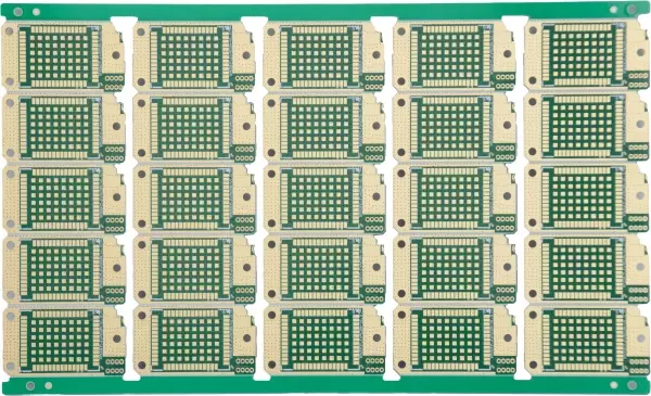
 Low-loss dielectric materials supporting frequencies up to tens of GHz
 Precision impedance control to minimize signal attenuation
 Requires tight tolerance in trace geometry and dielectric consistency
 Excellent signal stability across wide temperature and frequency ranges
 Used in 5G base stations, radar systems and RF antennas

| Feature | Technical specification |
| Number of layers | 4-20 Layers |
| Materials | Low loss / low Dk, higher performance FR-4, PPO, Teflon, hydrocarbon / ceramic filled |
| Copper weights (finished) | 0.5 oz – 6 oz |
| PCB Thickness | 0.40 mm – 6.0 mm |
| Max. dimensions | 620 mm x 720 mm |
| Min. track and gap | 0.075 mm / 0.075 mm |
| Min. mechanical drill | 0.15 mm |
| Surface finishes available | HASL (SnPb), LF HASL (SnNiCu), OSP, ENIG, Immersion Tin, Immersion Silver, Electrolytic gold, Gold fingers |
![]()
Engineering Support
![]()
Prototyping Services
![]()
Fast Turnaround
![]()
Seamless Transition to Mass Production
 Are high-frequency PCBs only for telecom products?
 No. They’re also used in automotive radar, medical equipment, satellite systems, and any product where signal quality at high speeds is critical.
 Do high-frequency PCBs require special testing or handling?
 Yes. They need precise manufacturing, tight tolerance control, and often stricter quality checks to ensure performance meets demanding specs.
 Why do I need a high-frequency PCB for my product?
 If your product needs to transmit signals fast and clearly—like in 5G, radar, or wireless devices—a high-frequency PCB helps maintain signal integrity, reduce signal loss, and ensure minimal interference.
 What materials are used in the manufacturing of High-Frequency PCBs?
 High-frequency PCBs are made using specialized laminates such as PTFE (Teflon), Rogers, and other low-loss materials. These materials are selected based on their dielectric constant, loss tangent, and thermal conductivity to ensure reliable performance at high frequencies.
 What makes High Frequency PCBs different from regular PCBs?
 High-frequency PCBs are designed to handle RF signals, which require precise impedance control, minimal signal loss, and low interference. Unlike regular PCBs, RF PCBs are made with materials that have specific electrical and thermal properties to perform reliably at high frequencies.
 What is a High Frequency PCB?
 A High-Frequency PCB is specifically designed for applications operating at RF and microwave frequencies, typically ranging from 3 MHz to 100 GHz. These boards are engineered to support high-speed signal transmission while minimizing losses.

Customer support