Introduction
In the heart of electronics manufacturing lies the PCB Factory — a hub where innovation meets rigorous engineering to create the backbone of today’s devices. At SprintPCB, our PCB manufacturing facility combines cutting-edge automation, ISO-certified processes, and a customer-centric approach to produce circuit boards trusted by industries from aerospace to medical tech. This guide takes you behind the scenes of a PCB factory, revealing how SprintPCB balances scale, precision, and sustainability to power your projects.
What Is a PCB Factory? The Engine of Electronics Innovation
A PCB Factory is a specialized facility designed for end-to-end production of printed circuit boards, encompassing:
- Core Processes: Design validation, material sourcing, fabrication, assembly, testing.
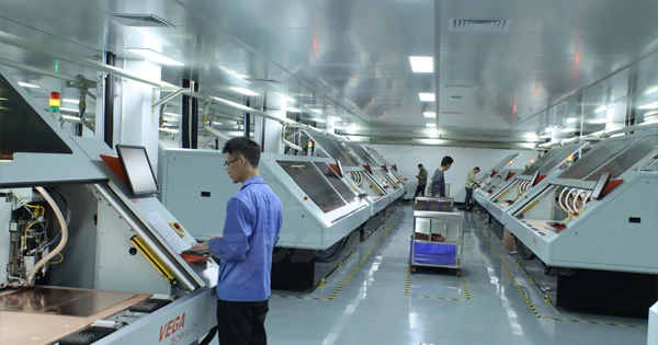
- Key Equipment: Automated optical inspection (AOI) systems, laser drilling machines, reflow ovens.
- Scale: High-mix, low-volume (HMLV) prototyping to mass production (10,000+ boards/day).
SprintPCB’s Facility Highlights:
- 15,000 sq. ft. factory with Class 1000 clean rooms.
- Dedicated lines for rigid, flex, and HDI PCBs.
- ERP-integrated workflow for real-time order tracking.
7 Reasons to Choose a Certified PCB Factory Like SprintPCB
- Advanced Automation: Robotic pick-and-place systems achieve 99.98% placement accuracy.
- Material Expertise: Partnerships with DuPont, Isola, and Rogers for high-frequency laminates.
- Rapid Turnaround: 24-hour prototyping and 5-day volume production.
- Quality Assurance: IPC-A-600 Class 3 standards for mission-critical boards.
- Cost Efficiency: Bulk material sourcing reduces pricing by 15–25%.
- Environmental Compliance: ROHS, REACH, and halogen-free production.
- Global Logistics: Door-to-door shipping with customs clearance support.
A Day in the Life of SprintPCB’s PCB Factory
Step 1: Design Validation
- Engineers review Gerber files for DFM (Design for Manufacturing) compliance.
- Signal integrity simulations using ANSYS HFSS.
Step 2: Panel Preparation
- Cutting FR-4, aluminum, or polyimide substrates into standardized panels.
- Laser direct imaging (LDI) for inner layer patterning.
Step 3: Etching & Layer Bonding
- Plasma etching to remove excess copper (tolerance ±2μm).
- Hydraulic lamination at 350 psi for multilayer boards.
Step 4: Drilling & Plating
- Laser drilling (50μm microvias) and mechanical drilling (0.15mm holes).
- Electroless copper deposition for through-hole conductivity.
Step 5: Solder Mask & Silkscreen
- LPI (Liquid Photo-Imageable) solder mask application via curtain coating.
- UV-cured silkscreen for component labels.
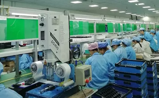
Step 6: Assembly & Testing
- SMT (Surface Mount Technology) lines place 25,000 components/hour.
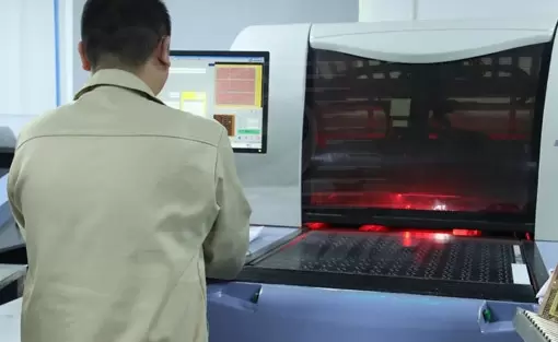
- X-ray inspection for BGA soldering and flying probe electrical testing.
How SprintPCB’s PCB Factory Tackles Industry-Specific Challenges
| Industry | Challenge | SprintPCB Solution |
| Medical | Biocompatible materials | ISO 13485-certified lines with medical-grade FR-4. |
| Automotive | High-temperature reliability | IATF 16949 processes, Tg170 substrates. |
| Aerospace | EMI/RFI shielding | 4-layer shielding with silver ink. |
| IoT | Ultra-thin designs | 0.2mm flex PCBs with roll-to-roll production. |
Quality Control in a PCB Factory: Beyond ISO Standards
SprintPCB enforces a 5-stage QC protocol:
- Incoming Material Check: XRF testing for copper purity and laminate thickness.
- In-Process Inspection: AOI verifies trace width/spacing (min. 3/3 mil).
- Electrical Testing: 100% continuity and insulation resistance checks.
- Environmental Stress Screening (ESS):
- Thermal cycling (-55°C to 125°C, 100 cycles).
- 85°C/85% RH humidity testing for 168 hours.
- Final Audit: Cross-functional team reviews documentation (IPC-6012 reports).
The Economics of PCB Factory Operations: Cost vs. Value
Labor Costs: Automation reduces manual labor by 60% vs. traditional factories.
Material Waste: Panel optimization software minimizes scrap (<5%).
Energy Consumption: Solar-powered facilities cut CO2 emissions by 30%.
ROI Case Study: A client reduced assembly defects by 40% after switching to SprintPCB’s factory.
Conclusion
Choosing the right PCB factory isn’t just about cost—it’s about partnering with a team that understands your technical, logistical, and regulatory needs. With SprintPCB, you gain access to scalable production, unwavering quality, and a roadmap for tomorrow’s innovations.
Ready to experience world-class PCB manufacturing? Contact SprintPCB today for a free factory tour or instant quote!