The Rise of Multilayer PCBs in Modern Electronics
In today’s electronics landscape, where compact and high-performance solutions are in demand, Multilayer PCBs have become essential for advanced circuitry. These intricate boards are found in everything from 5G infrastructure to medical imaging systems, allowing engineers to pack more functionality into smaller spaces. At SprintPCB, we excel in Multilayer PCB fabrication, combining precision engineering with unmatched reliability. This guide delves into design fundamentals, manufacturing processes, and cutting-edge trends, empowering you to fully utilize Multilayer PCB technology.
Understanding Multilayer PCBs: Beyond Basic Simplicity
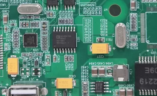
A Multilayer PCB integrates three or more conductive copper layers, separated by insulating dielectric material and bonded under heat and pressure. These layers are interconnected through plated through-holes (PTHs) or microvias, making them ideal for complex devices such as:
- Consumer Electronics: Smartphones featuring 10+ layer boards for 5G antennas.
- Industrial Automation: Motor controllers with integrated thermal management.
- Aerospace: Avionics systems requiring EMI shielding and high-speed signal integrity.
Why Multilayer PCBs Outperform Single/Double-Layer PCBs:
- Space Efficiency: 50–70% smaller footprint compared to equivalent single-layer designs.
- Improved Signal Quality: Dedicated ground/power planes reduce noise interference.
- Enhanced Durability: Laminated FR-4 cores withstand vibration and thermal cycling.
Six Industries Transformed by Multilayer PCBs
Telecommunications: 12–20 layer PCBs power 5G base stations and millimeter-wave routers.
Medical Devices: Flexible Multilayer PCBs enable MRI machines and portable health monitors.
Automotive: ADAS (Advanced Driver Assistance Systems) rely on HDI (High-Density Interconnect) boards.
IoT: Ultra-thin 6-layer designs drive smart sensors and wearable technology.
Defense: Ruggedized boards support radar systems and secure communication devices.
Energy: Multilayer PCBs are crucial for solar inverters and battery management systems (BMS).
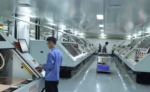
The Precision Manufacturing Process of Multilayer PCBs at SprintPCB
Our Multilayer PCB production meets IPC-6012 Class 3 standards, ensuring the highest quality:
Layer Stackup Design
- Optimize layer arrangement for impedance control, such as signal-ground-signal configurations.
- Select materials: High-Tg FR-4, Rogers 4350B, or polyimide for flex-rigid hybrids.
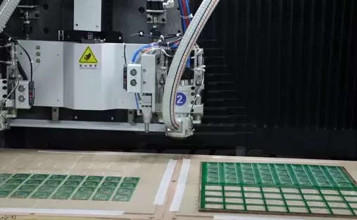
Inner Layer Imaging
- Laser direct imaging (LDI) achieves 25μm line/space accuracy for precise patterns.
- AOI (Automated Optical Inspection) detects defects before lamination for quality assurance.
Lamination & Drilling
- Hydraulic presses bond layers at 180°C and 350 psi for strong adhesion.
- Laser drilling creates microvias (50–100μm diameter) in HDI boards for complex connections.
Plating & Surface Finish
- Electroless nickel immersion gold (ENIG) provides excellent corrosion resistance.
- Via filling with conductive epoxy prevents air pockets for reliable electrical connections.
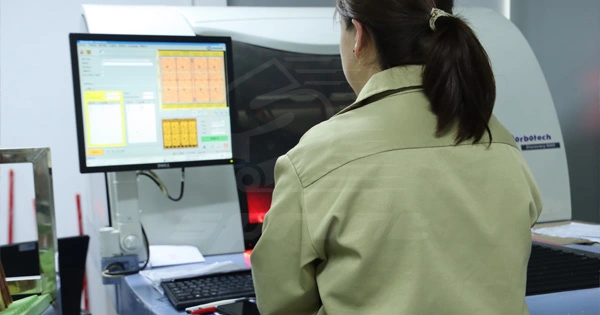
Final Testing
- TDR (Time-Domain Reflectometry) verifies impedance for high-speed signal integrity.
- Thermal shock testing (-55°C to 125°C, 500 cycles) ensures durability in extreme conditions.
Five Essential Best Practices for Multilayer PCB Design
- Early Layer Stackup Planning: Separate analog and digital grounds to prevent noise coupling. Utilize symmetrical stacking to avoid warping (e.g., 4-layer: Signal-GND-PWR-Signal).
- Signal Integrity Management: Route high-speed traces (e.g., DDR4, PCIe) on adjacent layers with ground shielding. Follow the 3W rule (trace spacing = 3x trace width) to minimize crosstalk interference.
- Effective Thermal Design: Place thermal vias under power components (e.g., QFN packages) for heat dissipation. Use copper pours on inner layers to manage heat efficiently.
- DFM Optimization: Avoid via-in-pad unless necessary, as it can increase costs by 15–20%. Ensure annular rings are ≥0.15mm for reliable drilling and plating.
- Collaboration with Your Manufacturer: Share Gerber, IPC-356, and ODB++ files for seamless Multilayer PCB fabrication. Validate stackup Tg (glass transition temperature) and CTE (thermal expansion coefficient) to prevent manufacturing issues.
Navigating Multilayer PCB Production Costs: Optimization Strategies
Layer Count: A 6-layer PCB typically costs ~40% more than a 4-layer board due to increased complexity and material usage.
Materials: High-frequency laminates like Rogers add 30–50% to costs compared to standard FR-4 materials.
Holes: Laser-drilled microvias cost $0.02–0.05 per hole, while mechanical drills cost only $0.005 per hole.
Lead Time: Expedited 5-day turnaround services may cost 25% more than standard 10-day production cycles.
SprintPCB’s Cost-Saving Tips:
- Use standard 1.6mm board thickness unless specific requirements dictate otherwise.
- Opt for HASL (Hot Air Solder Leveling) finish for non-critical applications to reduce costs.
- Panelize small boards to minimize material waste and maximize production efficiency.
Multilayer PCB vs. HDI: Choosing the Right Technology for Your Project
| Factor | Multilayer PCB | HDI PCB |
| Layers | 4–16 layers | 8–20+ layers with microvias |
| Line/Space | 100/100μm | 50/50μm or finer |
| Applications | Industrial controls, power supplies | Smartphones, military radios |
| Cost | $0.50–$5/sq. inch | $2–$10/sq. inch |
Looking Ahead: Innovations in Multilayer PCB Technology
- Embedded Passives: Resistors and capacitors integrated into inner layers, reducing surface area by up to 30%.
- 3D Printed Electronics: Additive manufacturing enables rapid prototyping of 8-layer boards.
- AI-Powered Design Tools: Auto-route complex BGA breakouts in minutes for faster design cycles.
- Sustainable Materials: Halogen-free laminates and recyclable copper cores promote eco-friendly electronics.
Why SprintPCB is the Leader in Multilayer PCB Manufacturing
- Advanced Capabilities: Support for up to 32 layers, 25μm laser drilling, and ±10% impedance control.
- Comprehensive Certifications: ISO 9001, AS9100 (aerospace), and IATF 16949 (automotive) ensure quality and compliance.
- Global Production Network: Seamless transition from prototype to volume production across US, EU, and Asia facilities.
- Dedicated Support: Our engineering team provides expert guidance for stackup design and DFM analysis.
Conclusion
From IoT wearables to satellite communications, Multilayer PCBs are driving innovation in electronics by enabling miniaturization and enhanced performance. Partner with SprintPCB to access our state-of-the-art fabrication processes, rigorous testing protocols, and unparalleled technical expertise.
Need a reliable Multilayer PCB supplier? Upload your design files today for a free quote and enjoy 15% off your first order!