In the realm of advanced electronics, Multilayer PCBs are indispensable for achieving compactness and high performance. This article delves into critical design considerations—stack-up configuration, signal integrity, and thermal management—that influence the functionality and reliability of Multilayer PCBs.
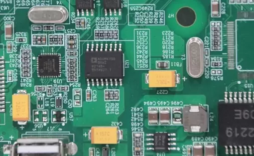
The stack-up of a Multilayer PCB determines its electrical performance and manufacturability. A well-planned stack-up minimizes electromagnetic interference (EMI) and ensures signal integrity. Key considerations include:
Alternating signal and ground/power planes can reduce crosstalk and EMI.
A symmetrical stack-up prevents warping during manufacturing.
Choosing appropriate dielectric materials affects impedance control and thermal performance.
For instance, incorporating dedicated ground planes adjacent to signal layers can significantly enhance signal return paths, thereby reducing noise.
Signal integrity is paramount in high-speed circuit designs. Factors affecting it include:
Maintaining consistent impedance prevents signal reflections.
Proper via placement and sizing reduce inductance and signal loss.
Short, direct routing paths minimize delay and distortion.
Implementing differential pair routing and controlled impedance traces are effective strategies to uphold signal integrity in complex Multilayer PCB designs.
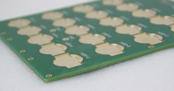
Effective thermal management ensures the longevity and reliability of electronic components. Techniques include:
These facilitate heat transfer from hot components to internal copper planes.
Attaching these to high-power components dissipates heat efficiently.
Using substrates with high thermal conductivity aids in heat distribution.
For example, integrating thermal vias beneath power components can significantly reduce localized heating, enhancing overall board performance.
Designing a Multilayer PCB requires meticulous attention to stack-up configuration, signal integrity, and thermal management. By addressing these areas, engineers can develop reliable, high-performance PCBs suitable for various applications.

Customer support