1. Definition of High-Frequency PCB
A high-frequency PCB refers to a specialized circuit board used in high-frequency (greater than 300MHz or wavelengths shorter than 1 meter) and microwave (greater than 3GHz or wavelengths shorter than 0.1 meters) applications. These boards are produced using either standard rigid PCB manufacturing methods on microwave substrates or specialized processes. Typically, high-frequency PCBs are defined as those with frequencies above 1GHz.
With the rapid advancement of science and technology, more devices are being designed for microwave frequencies (>1GHz) and even millimeter-wave applications (>30GHz). This trend demands higher performance from PCB substrates. For instance, base materials must have excellent electrical properties and chemical stability, with minimal signal loss at increasing frequencies, highlighting the importance of high-frequency PCB materials.
2.1 Mobile communication products
2.2 Power amplifiers and low-noise amplifiers
2.3 Passive components such as power dividers, couplers, duplexers, and filters
2.4 Automotive collision avoidance systems, satellite systems, and radio systems. The trend of high-frequency electronics is growing.
3. Types of High-Frequency PCBs
3.1 Powder Ceramic-Filled Thermoset Materials
A. Manufacturers:
Rogers Corporation: 4350B/4003C
Arlon: 25N/25FR
Taconic: TLG series
B. Processing Methods:
Similar to FR4 (epoxy resin/glass fabric) processes, but the material is more brittle, prone to cracking, and requires special handling during drilling and milling, reducing tool life by 20%.
3.2 PTFE (Polytetrafluoroethylene) Materials
A. Manufacturers:
Rogers Corporation: RO3000 series, RT series, TMM series
Arlon: AD/AR series, IsoClad series, CuClad series
Taconic: RF series, TLX series, TLY series
Taixing Microwave: F4B, F4BM, F4BK, TP-2
B. Processing Methods:
1. Cutting:
Protect the material with a film to prevent scratches and dents.
2. Drilling:
Use new drill bits (standard 130) for best results, drill one panel at a time, and apply a 40psi pressure foot.
Cover with aluminum sheet, use a 1mm melamine pad to clamp the PTFE board.
Blow out dust from holes with an air gun after drilling.
Use the most stable drill machine with optimized parameters (smaller holes require faster drill speed, lower chip load, and slower retraction speed).
3. Hole Treatment:
Plasma treatment or sodium naphthalene activation to facilitate metallization.
4. PTH Copper Deposition:
Post-micro-etch (control at 20 microinches), start processing from the degreasing tank in the PTH line.
If needed, a second PTH pass may be performed, starting from the expected tank.
5. Solder Mask:
Pre-treatment with acid cleaning, avoiding mechanical scrubbing.
Bake after pre-treatment (90°C for 30 minutes), apply and cure solder mask.
Bake in three stages: 80°C, 100°C, and 150°C for 30 minutes each. If there is oil rejection, rework by stripping the solder mask and reactivating the surface.
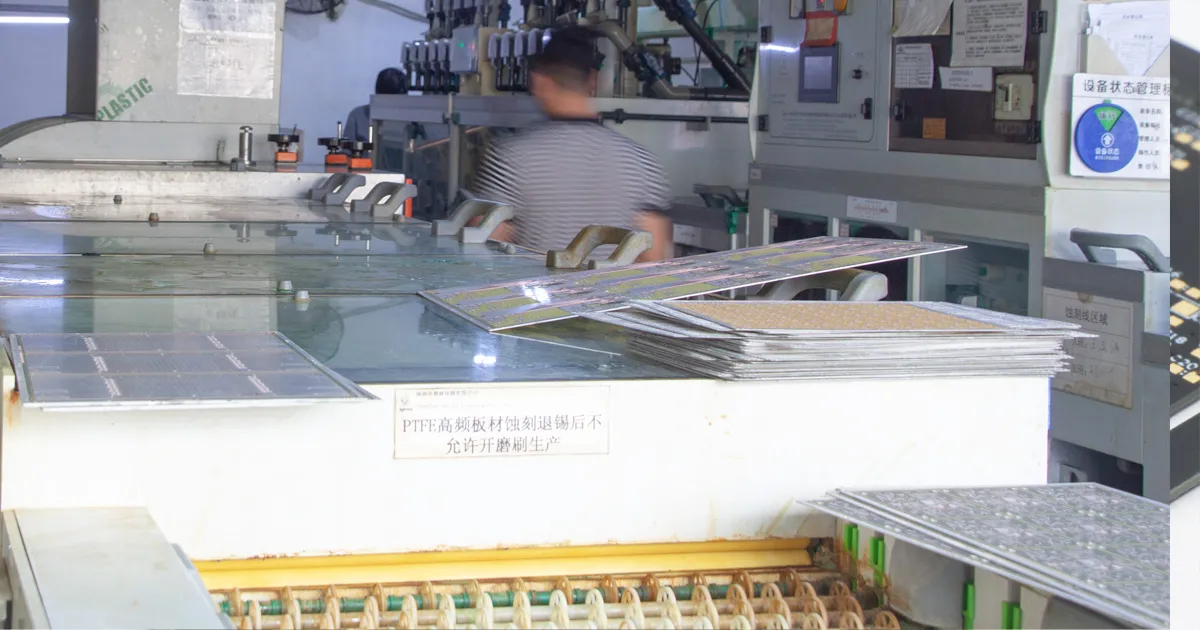
6. Milling:
Stack PTFE boards with protective paper on the circuit surface, clamped between etched copper-free FR-4 or phenolic baseboards (1.0mm thick).
After milling, carefully deburr edges by hand, avoid damaging the substrate and copper surface, and separate layers with sulfur-free paper for inspection.
4. Process Flow
1. NPTH PTFE Board Processing Flow:
Cutting → Drilling → Dry Film → Inspection → Etching → Etch Inspection → Solder Mask → Silkscreen → Tin Plating → Shaping → Testing → Final Inspection → Packaging → Shipping
2. PTH PTFE Board Processing Flow:
Cutting → Drilling → Hole Treatment (Plasma or Sodium Naphthalene Activation) → Copper Deposition → Electroplating → Dry Film → Inspection → Pattern Plating → Etching → Etch Inspection → Solder Mask → Silkscreen → Tin Plating → Shaping → Testing → Final Inspection → Packaging → Shipping
5. Challenges in High-Frequency PCB Processing
1. Copper Deposition: Difficulty in achieving copper adhesion on hole walls.
2. Pattern Transfer, Etching, and Line Width Control: Managing line width gaps and sand holes.
3. Solder Mask Process: Ensuring solder mask adhesion and controlling bubbling.
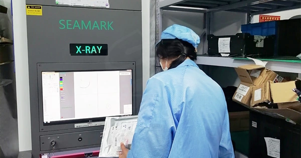
4. Surface Handling: Strict control to prevent scratches across various processes.
SprintPCB is a leading provider in the high-frequency PCB industry. Our advanced manufacturing techniques and high-quality materials ensure exceptional performance and reliability in high-frequency applications. Whether you are developing mobile communication devices, automotive systems, or any high-frequency electronics, SprintPCB offers tailored solutions to meet your needs.
Why Choose SprintPCB for High-Frequency PCBs?
Cutting-Edge Technology: We utilize the latest technology and equipment to manufacture high-frequency PCBs, ensuring superior performance.
Expertise: Our team of experts has extensive experience in handling high-frequency materials and processes.
Quality Assurance: Rigorous quality control measures are in place to ensure each PCB meets the highest standards.
Custom Solutions: We offer customizable solutions to cater to the specific requirements of your projects.
For more information on our high-frequency PCB solutions, visit
SprintPCB and discover how we can help you achieve excellence in your high-frequency applications.