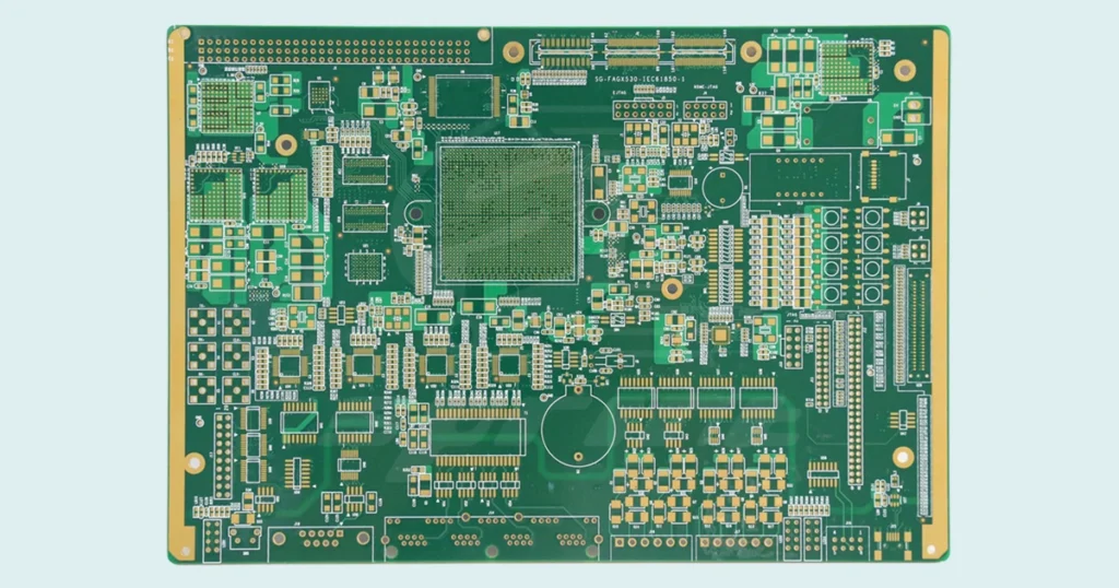
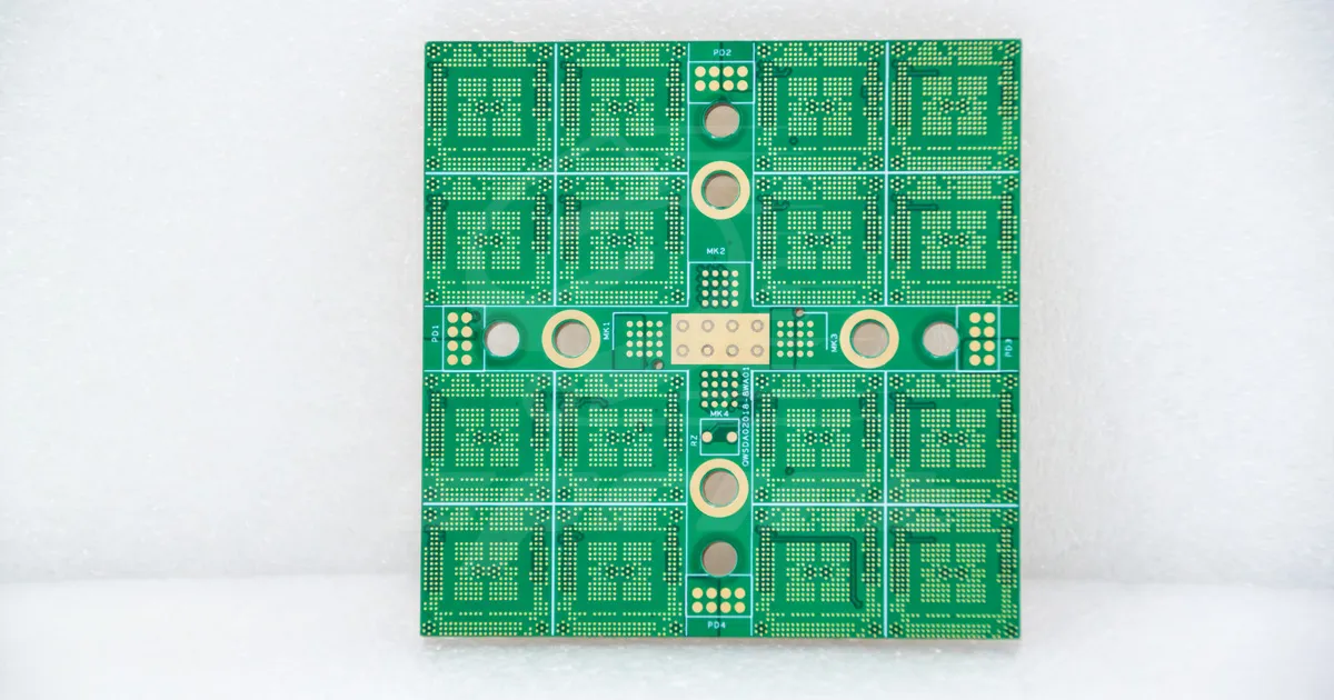
High Density Interconnect Printed Circuit Board (HDI PCB) is a new trend in the electronics industry. They use tiny lines and tiny apertures, allowing more components to be installed in less space. Here is some important information about HDI PCBs. HDI PCB has higher circuit density, smaller apertures and thinner circuits. This allows them to fit more components into a smaller space, thereby increasing the performance and functionality of the device. The manufacturing process of HDI PCB is more complex than traditional PCB. It requires the use of advanced equipment and technology, such as laser drilling, microcircuit pattern making, etc. This process requires precision and expertise to ensure the quality and performance of the final product. Due to its high density and high performance, HDI PCB is widely used in various high-end electronic devices, such as smartphones, tablets, medical equipment, etc.

Customer support