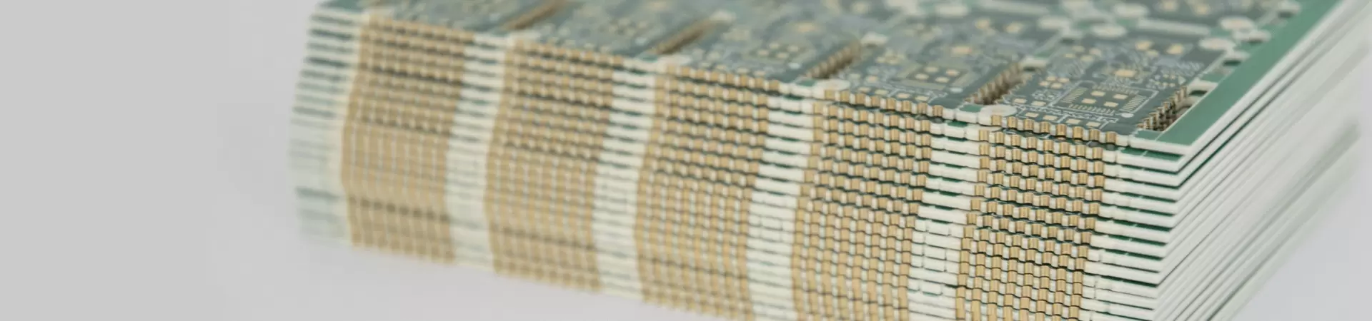
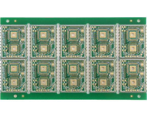
Metallized Half-Hole PCB
Metallized Half-Hole PCB is widely applied in telecommunication systems, especially RF modules, antenna circuits, microwave devices, and high-speed signal processing units.
Metallized Half-Hole PCB is widely applied in telecommunication systems, especially RF modules, antenna circuits, microwave devices, and high-speed signal processing units.
 Material: Hybrid stack-up RO4350 + FR4
Special Process: Metallized Half-Hole
Surface Finish: ENIG 0.05 μm
Board Thickness: 1.6 mm
Application: Telecommunications
| Feature | Technical specification |
| Number of layers | 2-40 Layers |
| Materials | FR-4 standard, FR-4 high performance, FR-4 halogen-free |
| Copper weights (finished) | 2oz – 6 oz |
| PCB Thickness | 0.40 mm – 6.0 mm |
| Max. dimensions | 620 mm x 720 mm |
| Min. track and gap | 0.075 mm / 0.075 mm |
| Min. mechanical drill | 0.15 mm |
| Surface finishes available | HASL (SnPb), LF HASL (SnNiCu), OSP, ENIG, Immersion Tin, Immersion Silver, Electrolytic gold, Gold fingers |
This PCB is built with a hybrid stack-up (RO4350 + FR4), combining the advantages of high-frequency materials and conventional FR4. The RO4350 ensures low dielectric loss and stable dielectric constant for high-speed and high-frequency signal transmission, while FR4 improves processability, mechanical reliability, and cost-effectiveness. This makes it ideal for designs requiring both performance and cost balance.
The metallized half-hole process enables modular design and small-board assembly, commonly used for reliable connections between RF/daughter boards and mainboards in telecommunication modules. This technique helps save board space, enhances assembly flexibility, and supports high-density interconnection requirements.
The ENIG surface finish (0.05 μm) provides a flat soldering surface with excellent conductivity and oxidation resistance, ensuring reliable solder joints. For RF communication applications where signal integrity and long-term stability are critical, ENIG significantly enhances reliability.
With a standard 1.6 mm thickness, the board maintains mechanical strength and compatibility with connectors and structural components in standardized assembly.
Thanks to its hybrid construction, metallized half-hole design, and ENIG finish, this PCB is widely applied in telecommunication systems, especially RF modules, antenna circuits, microwave devices, and high-speed signal processing units.

Engineering Support

Prototyping Services

Fast Turnaround

Seamless Transition to Mass Production
 Are there any design guidelines for thick copper PCBs? Can SprintPCB produce multilayer thick copper PCBs? What are the advantages of thick copper PCBs? What are the main applications of thick copper PCBs? What is considered a thick copper PCB? What quality issues should I watch for with thick copper PCBs?
 Pay attention to trace width, layer adhesion, and heat management. Work with an experienced manufacturer to avoid defects like uneven plating.

Customer support