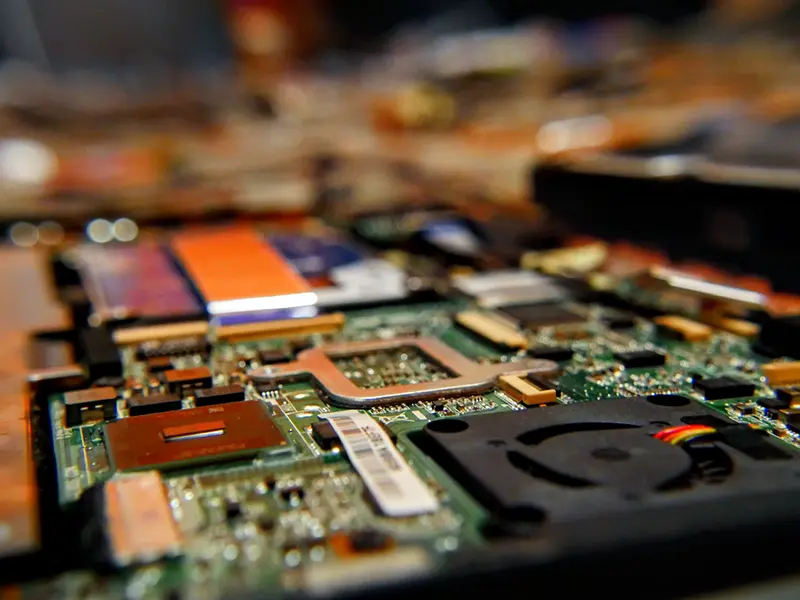
In the world of high-frequency electronics, RF PCB boards play a crucial role in maintaining signal integrity, minimizing losses, and ensuring the proper transmission of high-speed signals. These specialized printed circuit boards are designed to handle radio frequency (RF) signals and are essential for applications in fields like wireless communication, radar, and 5G networks. The selection of materials and the implementation of precision impedance control are two critical aspects of RF PCB board design that directly affect their performance. This article SprintPCB delves into the importance of material selection and precision impedance control when designing RF PCBs, highlighting how these factors impact the functionality and reliability of high-frequency systems.

The material used for an RF PCB board is the foundation for its ability to effectively handle high-frequency signals. The characteristics of the material directly influence the board's performance, such as its ability to minimize signal loss, maintain consistent impedance, and withstand various environmental conditions. Key material properties to consider when selecting an RF PCB board include dielectric constant (Dk), loss tangent (Df), and thermal stability.
Dielectric Constant (Dk): The dielectric constant measures a material's ability to store electrical energy in an electric field. In RF PCB boards, the lower the dielectric constant, the better, as it results in less signal delay and lower signal attenuation. A consistent Dk across the material is essential for maintaining signal integrity at high frequencies.
Loss Tangent (Df): The loss tangent measures how much energy is lost as heat within the material when a signal passes through it. RF PCBs require materials with a low loss tangent to minimize signal degradation. Higher losses can cause unwanted attenuation and impact the overall performance of the RF system.
There are several materials that are commonly used in the construction of RF PCB boards, each with distinct advantages depending on the specific application:
FR-4: While widely used in general PCB applications, FR-4 is not ideal for high-frequency RF PCB boards due to its relatively high dielectric constant and loss. For lower-frequency applications, FR-4 is acceptable, but for high-performance RF circuits, materials with better properties are recommended.
PTFE (Teflon): PTFE is a preferred material for high-frequency RF PCB boards due to its low dielectric constant and low loss tangent. These properties make PTFE highly suitable for applications in wireless communication, radar systems, and satellite technology. Additionally, PTFE offers excellent thermal stability, which is crucial for RF circuits exposed to high temperatures.
Ceramic-Filled Materials: Ceramic-filled materials provide a good balance between low dielectric constant, low loss, and high thermal stability. These materials are often used in microwave and radar applications where precise impedance control and high-frequency performance are critical.
Polyimide: Polyimide offers excellent thermal stability and low loss, making it a suitable choice for flexible RF PCB boards or applications that require flexibility without sacrificing performance. It is often used in flexible circuits for RF applications that require bending or shaping.
Impedance control is one of the most crucial aspects of RF PCB board design. In high-frequency circuits, maintaining a consistent impedance ensures that signals travel smoothly across the board, without interference or reflections. Impedance mismatches can lead to signal degradation, reduced efficiency, and system failure. Therefore, precision impedance control is essential for ensuring the proper functioning of RF systems.
For an RF PCB board to perform optimally, the impedance of the traces and components must be precisely controlled. Impedance mismatches cause reflections, which can lead to signal loss, noise, and even system malfunctions. Impedance control ensures that signals are transmitted without distortion, preserving the quality of high-frequency signals.
Impedance control is one of the most crucial aspects of designing an RF PCB board, as it directly impacts signal integrity and performance. There are two primary types of impedance to consider in RF PCB board design: characteristic impedance and differential impedance.
Characteristic impedance refers to the impedance that a transmission line, such as a trace on the RF PCB board, exhibits to an RF signal. It is essential to control this impedance precisely to ensure that the signal is transmitted without reflections or signal loss. The most common target impedances for RF PCBs are 50Ω for microstrip traces and 75Ω for coaxial traces. These values are typically used in applications such as antenna circuits, transmission lines, and wireless communication systems. Accurate characteristic impedance control ensures that the signal flows efficiently, maintaining the quality and strength of the transmitted data.
Differential impedance is critical for high-speed data transmission, where two conductors carry equal but opposite signals. In RF PCB boards, differential impedance refers to the impedance between these two conductors. It is commonly used in applications such as USB, Ethernet, and other high-speed digital communication systems. For these systems, maintaining a balanced differential impedance is vital to minimize noise and ensure reliable data transfer. Differential impedance helps to maintain signal integrity in environments where data transmission speeds are high, ensuring that the signals arrive at their destination without degradation.
Achieving precise impedance control in RF PCB boards requires careful design and the application of several strategies. The goal is to ensure that the impedance remains consistent across the PCB to maintain signal integrity. Here are the primary methods used to achieve precision impedance control in RF PCB boards:
The width of the traces and the spacing between the traces and the reference planes are crucial factors that influence impedance. For RF PCB boards, the correct trace width and spacing must be calculated based on material properties, the desired impedance (such as 50Ω or 75Ω), and the frequency of operation. Any variation in the width or spacing can lead to impedance mismatch, causing signal reflection, loss, or distortion. Accurate trace width and spacing design is critical for ensuring that the RF PCB board maintains the correct impedance for optimal signal transmission.
The arrangement of the PCB layers, known as the stack-up, plays a significant role in maintaining impedance control. For multi-layer RF PCBs, the positioning of signal layers relative to ground and power layers is essential for controlling the impedance. In some designs, the inner layers of the PCB can serve as reference planes for the signal traces. This layer configuration helps maintain consistent impedance throughout the PCB and minimizes the risk of impedance variations. A well-designed stack-up ensures stable signal transmission and reduces the chances of signal interference or degradation.
In RF PCB boards, microstrip traces and stripline traces are commonly used for impedance control. Microstrip traces are placed on the outer layers of the PCB with a reference ground plane beneath them. These are typically used for single-ended signal transmission. For more precise impedance control, stripline traces are used. Stripline traces are sandwiched between two reference planes and are generally employed in multi-layer designs. Stripline configurations provide better impedance stability, especially at higher frequencies, and are often used for critical high-frequency circuits in RF PCB boards.
Modern PCB design tools and simulation software have revolutionized the process of achieving precise impedance control. By using advanced simulation software, designers can model the impedance characteristics of their RF PCB boards before manufacturing. This allows them to optimize parameters such as trace width, spacing, and layer stack-up to achieve the desired impedance. Simulation tools can also predict how the PCB will perform in real-world conditions, enabling designers to make adjustments before the board is physically produced. This capability significantly reduces the risk of impedance mismatches and signal integrity issues in the final product.
The material of the RF PCB board has a significant impact on impedance control. Materials with a consistent dielectric constant, such as PTFE and ceramic-filled compounds, help maintain stable impedance across the board. Any variation in dielectric constant can lead to fluctuations in impedance, which can cause signal degradation or loss. By using high-quality, consistent materials, RF PCB boards can maintain precise impedance, ensuring high signal integrity.
Selecting the right material and achieving precise impedance control in an RF PCB board design are not without challenges. High-performance materials such as PTFE and ceramic-filled compounds, while essential for optimal performance, are often more expensive than standard FR-4. This price difference can make cost a significant consideration for many RF PCB board designs, especially in large-scale or budget-conscious projects.
In addition to material selection, achieving precise impedance control is another complex aspect of designing RF PCBs. Maintaining a stable and consistent impedance across the PCB is critical to ensure signal integrity, but it requires careful design and advanced simulation tools. Any deviation in impedance can result in signal reflections, loss, or distortion, which is especially detrimental in high-frequency applications.
Thermal management also presents a challenge when working with RF PCB boards. These circuits typically operate at high frequencies, which generate heat that can negatively impact their performance. Proper heat dissipation is crucial to prevent signal loss due to overheating, making it essential to select materials with high thermal conductivity and implement efficient cooling solutions. Without addressing thermal concerns, the reliability of the RF PCB board could be compromised, leading to degraded performance or even failure in critical applications.
The selection of the right material and the implementation of precision impedance control are crucial for the performance of RF PCB boards. The choice of material influences the board's ability to handle high-frequency signals with minimal loss, while precise impedance control ensures that signals are transmitted without distortion. By carefully selecting materials with low dielectric constants and low loss tangents, and by employing effective impedance control techniques, designers can ensure that their RF PCB boards will deliver superior performance in demanding applications such as 5G communication, radar systems, and wireless devices. Understanding these critical factors is key to achieving high-quality, reliable RF designs.

Customer support