As electronic systems continue advancing into the era of high-speed processing, smart connectivity, and ultra-compact product design, engineers are facing increasing challenges in achieving both functional density and long-term reliability. The multilayer PCB has become the cornerstone technology enabling this transformation. By incorporating multiple conductive layers in a precisely engineered stack-up, multilayer PCB solutions allow designers to integrate complex digital, analog, and RF circuits within limited space—while maintaining stable power delivery and superior signal performance. This article explores why multilayer PCB has become indispensable in modern electronics and the essential engineering factors that influence its success from concept to manufacturing.

As modern electronics continue evolving toward smaller sizes and stronger computing capabilities, the multilayer PCB has become a critical foundation of advanced system architecture. Whether in consumer electronics or aerospace equipment, a well-engineered multilayer PCB ensures higher performance, optimized signal routing, and reliable power delivery in compact spaces—something that traditional single-layer or double-layer boards can no longer achieve.
The increasing need for lightweight and portable products drives the adoption of multilayer PCB technology. By stacking multiple conductive layers separated by insulation, designers can implement far more complex circuitry without increasing board dimensions. This high-density layout supports wearable electronics, medical implants, and compact IoT systems, allowing devices to handle sophisticated functions within miniature form factors.
A multilayer PCB provides dedicated signal, ground, and power layers that improve electrical performance dramatically:
Reduced noise and interference in RF and high-speed digital signals
Controlled impedance routing for stable data transmission
Lower crosstalk thanks to the separation of sensitive analog and digital paths
These improvements are essential for 5G networking equipment, AI computing boards, and advanced automotive electronics where reliability at high frequency is mandatory.
Complex electronics often require stable voltage delivery and effective heat control. The structure of a multilayer PCB enables efficient power plane configuration:
Optimized power distribution networks reduce voltage drop
Copper balancing helps dissipate heat uniformly
Better current-carrying capacity for high-power modules
This makes multilayer PCB solutions a preferred choice for EV power systems, industrial control units, and high-performance servers.
As products diversify, engineers need more flexible circuit architecture. Multilayer PCB manufacturing supports:
Blind/buried vias and HDI mini-vias
Integration of RF, analog, and digital in a single board
Rigid-flex multilayer structures for dynamic environments
These capabilities push forward innovations in robotics, UAVs, and space-constrained defense technology.
When developing high-performance electronic systems, engineers must pay close attention to design parameters that directly affect the reliability and manufacturability of a multilayer PCB. As devices become more compact and communication speeds increase, multilayer PCB design requires strategic optimization from layout to production. Understanding the key considerations below helps ensure smooth engineering validation and successful mass manufacturing.
The structure of a multilayer PCB is defined by its stack-up configuration. Proper arrangement of signal, ground, and power layers ensures stable performance:
Symmetrical stack-up reduces warpage during reflow processes
Accurate dielectric thickness supports impedance control
Ground planes must be placed near high-speed signal layers to minimize noise
A well-designed stack-up enhances both signal integrity and mechanical reliability.
In multilayer PCB high-speed applications, maintaining clean signals is critical. Engineers should consider:
Differential pair routing for stability in high-frequency channels
Controlled impedance lines to reduce reflections and distortions
Minimizing via transitions to avoid signal loss
These strategies support 5G systems, automotive radar modules, and advanced computing electronics.
Modern electronic components generate significant heat. A multilayer PCB enables multiple heat dissipation pathways:
Thicker copper for power layers improves current handling
Thermal vias help transfer heat to heat sinks or metal cores
Balanced copper distribution prevents localized hot spots
Effective power delivery and thermal control extend product lifespan in demanding environments.
To route signals between internal layers, engineers must select appropriate via structures:
Blind and buried vias for high-density interconnects
Microvias for HDI multilayer PCB designs
Via-in-pad for compact BGA packages
Manufacturability should always be reviewed with the PCB supplier early to prevent costly re-spins.
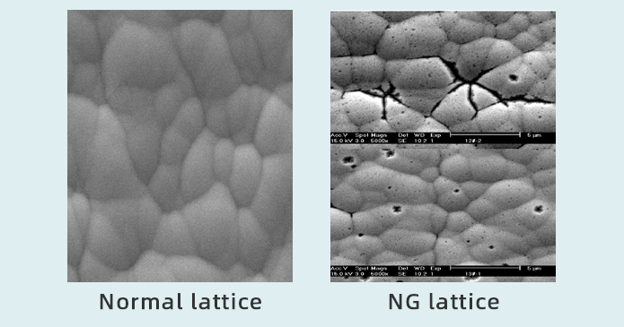
Choosing the right materials ensures that the multilayer PCB can withstand environmental and mechanical stresses:
Low-loss laminates for high-speed RF
High-TG materials for elevated operating temperatures
Strict reliability testing (thermal cycling, solderability, CAF resistance)
High-quality materials improve long-term stability in automotive, aerospace, and industrial devices.
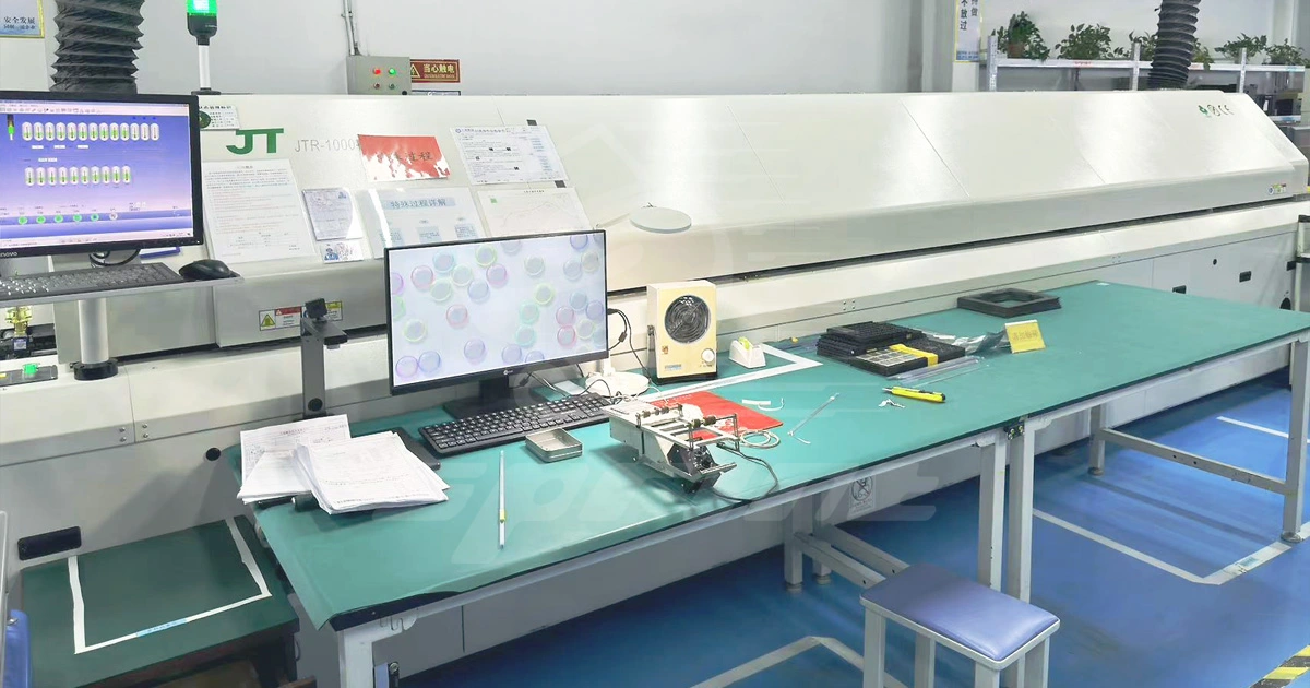
SprintPCB multilayer PCB solutions support 4–60 layers, enabling ultra-high routing density and stable performance in compact electronic systems. With excellent signal integrity and electromagnetic compatibility, these multilayer PCB products are manufactured in SprintPCB's advanced factories using precision engineering processes. Key capabilities include blind and buried vias, via-in-pad, backdrilling, impedance control, and copper thickness options from 0.5 OZ to 6 OZ. SprintPCB offers high-performance FR4, halogen-free, and low-loss materials, board sizes up to 620 mm × 720 mm, and fine line widths down to 0.075 mm—meeting the reliability requirements of servers, network infrastructure, and high-end medical equipment. From rapid prototyping to volume production, SprintPCB ensures consistent quality and faster time-to-market for multilayer PCB board innovation.
The evolution of advanced electronics depends heavily on how efficiently signals, power, and thermal loads are managed inside the hardware. A well-designed multilayer PCB not only boosts system performance but also supports innovation across industries—from consumer smart devices and EV systems to aerospace and defense technologies. By focusing on correct stack-up planning, signal integrity control, thermal management, manufacturability, and material reliability, engineers can unlock the full potential of multilayer PCB technology. Looking ahead, the multilayer PCB will remain a key enabler of next-generation electronic products that are faster, smaller, and more powerful than ever.

Customer support