In today's electronics industry, the push for smaller, lighter, and more powerful devices has never been stronger. Every new generation of smartphones, tablets, wearables, and networking equipment requires higher performance in an even smaller footprint. At the heart of this evolution lies the HDI PCB board—a cutting-edge technology that makes it possible to integrate more functions into compact designs while still maintaining signal integrity and overall reliability.
Unlike traditional printed circuit boards, an HDI PCB board is specifically designed to support ultra-dense circuitry. By incorporating fine lines, microvias, buried vias, and advanced stack-ups, it provides engineers with the freedom to design next-generation electronics without the limitations of conventional PCB technology. As demand for miniaturization continues to rise, choosing the right HDI PCB board supplier becomes a strategic decision that directly impacts product performance, production costs, and time-to-market.

An HDI PCB board stands out because of its ability to deliver exceptional performance in a minimal amount of space. The technology goes beyond just shrinking down components—it is about rethinking how signals are routed, how vias are formed, and how multiple layers can be stacked for maximum efficiency.
The uniqueness of HDI technology comes from a combination of several advanced design features:
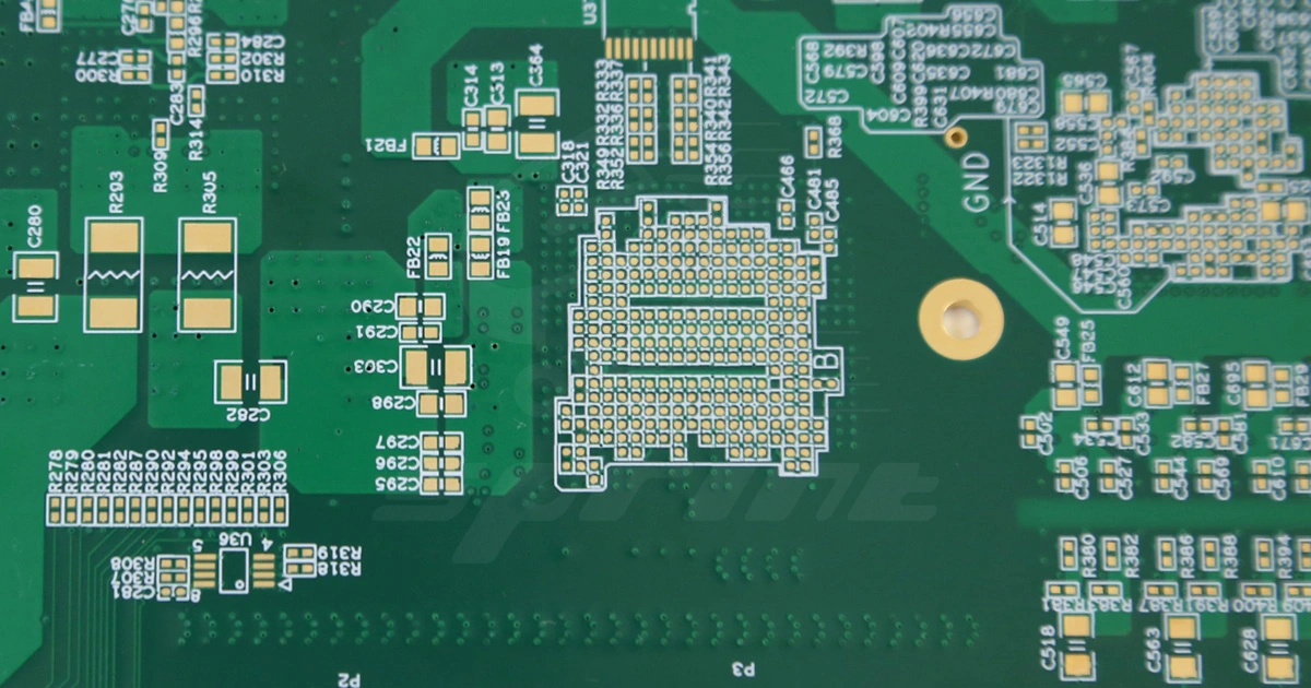
Microvia Technology: Instead of large mechanical drill holes, HDI PCB boards use laser-drilled microvias. These vias can be as small as 0.10 mm (and even 0.075 mm in advanced builds), reducing unnecessary stubs and enabling more effective layer-to-layer connections. The result is faster signal transmission and improved electrical performance.
Fine Line and Space: Traditional PCBs typically struggle to handle line widths and spacing smaller than 0.15 mm. In contrast, HDI PCB boards produced by SprintPCB achieve line/space as fine as 0.075 mm. This capability is essential when designing high-speed circuits where routing density must be maximized without compromising quality.
Advanced Stack-Ups: HDI PCB boards can be manufactured in 1+N+1, 2+N+2, 3+N+3, and even 4+N+4 structures. This flexibility allows engineers to integrate blind and buried vias in a way that minimizes board thickness while supporting complex designs. For demanding projects, SprintPCB even develops any-layer HDI technology.
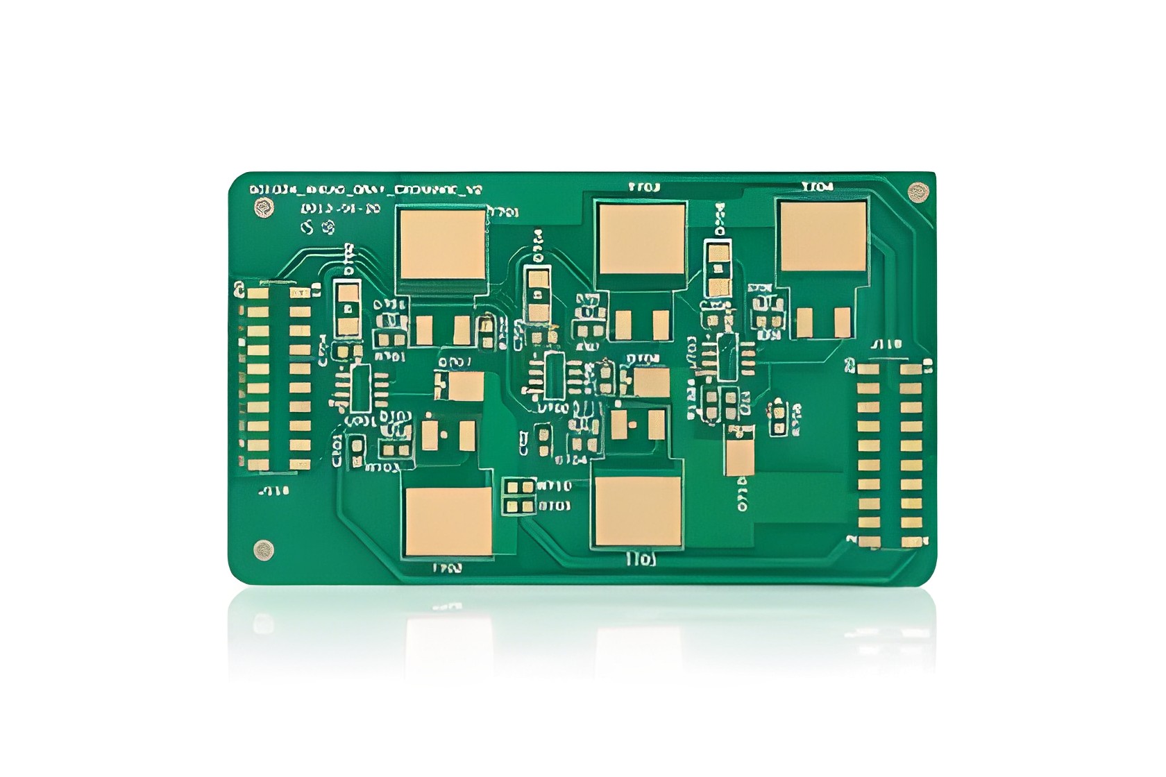
Compact Yet Reliable: One of the main advantages of an HDI PCB board is that it supports higher circuit density while reducing the size and weight of the overall product. Despite being thinner and lighter, SprintPCB ensures these boards maintain long-term durability and consistent performance.
These attributes make HDI PCB boards indispensable in industries such as consumer electronics, automotive systems, aerospace, defense, and medical devices—anywhere that compactness, reliability, and high performance are mandatory.
This is where SprintPCB plays a vital role. With proven expertise and advanced manufacturing capabilities, SprintPCB delivers HDI PCB boards that meet the most demanding requirements of high-speed, compact, and mission-critical electronic applications.
When it comes to HDI PCB board production, not every manufacturer can deliver the precision and consistency required for advanced electronics. SprintPCB distinguishes itself through state-of-the-art equipment, experienced engineers, and a proven track record of serving global clients.
SprintPCB invests heavily in precision technologies to achieve the high-density interconnect requirements demanded by modern designs. Laser drilling machines ensure microvias are consistent and reliable. Automated plating processes guarantee robust connections between layers. Meanwhile, high-resolution imaging systems allow SprintPCB to achieve fine line/space tolerances that many manufacturers cannot match.
The company's ability to produce HDI PCB boards with up to 60 layers provides unmatched design flexibility. Whether a project requires a simple 4-layer prototype or a complex 4+N+4 HDI stack-up for advanced telecom equipment, SprintPCB can deliver.
Different applications require different material properties. SprintPCB offers a wide range of base materials including high-performance FR4 for general applications, halogen-free FR4 for environmentally conscious designs, and Rogers materials for high-frequency and RF projects. This flexibility ensures that customers can select the ideal balance of cost, performance, and compliance for their HDI PCB board needs.
The surface finish of an HDI PCB board plays a crucial role in solderability, oxidation resistance, and long-term reliability. SprintPCB provides multiple finishes such as ENIG (Electroless Nickel Immersion Gold), immersion silver, immersion tin, HASL, LF HASL, and gold fingers. By offering this variety, SprintPCB ensures customers can choose the finish most suitable for their assembly and end-use requirements.
The HDI PCB board is essential for compact, high-performance electronics, offering superior density, reliability, and signal integrity. With advanced technologies like laser-drilled microvias, fine line/space, and multi-layer stack-ups, SprintPCB delivers boards that meet the toughest design and production requirements. For businesses seeking a trusted partner in HDI PCB board manufacturing, SprintPCB provides the precision, speed, and support needed to bring innovative products to market successfully.

Customer support