In the era of smart devices and interconnected systems,
PCB HDI (High-Density Interconnect) technology stands at the forefront of innovation. By enabling engineers to pack more functionality into smaller spaces while enhancing speed and reliability, HDI PCBs are redefining industries from healthcare to aerospace. At SprintPCB, we combine cutting-edge
PCB HDI expertise with decades of manufacturing excellence to deliver solutions that power tomorrow’s breakthroughs. This 1800-word guide dives into the world of HDI technology, exploring its design principles, applications, and how SprintPCB is shaping the future of electronics.
Understanding PCB HDI: The Engine Behind Modern Electronics
PCB HDI refers to advanced circuit boards designed with ultra-fine traces, microvias, and high-layer counts to achieve unparalleled density and performance. These boards are critical for devices where size, weight, and signal integrity are paramount.
Key Features of HDI Technology
- Microvias: Laser-drilled holes (as small as 50µm) replace traditional through-holes, saving space and reducing signal loss.
- Stacked and Staggered Vias: Enable complex interconnections in multilayer designs.
- Thin Materials: Ultra-slim substrates (e.g., 25µm cores) for lightweight, flexible applications.
- Any-Layer Build-Up: Eliminates layer constraints, allowing circuits to be built vertically and horizontally.
SprintPCB’s PCB HDI solutions are trusted by global leaders in 5G, IoT, and medical technology, where precision and reliability are non-negotiable.
Designing for Success: The PCB HDI Development Process
Creating high-density boards demands a blend of innovation and meticulous execution. Here’s how SprintPCB ensures excellence:
Collaborative Design Strategy
- Requirements Analysis: Our engineers work closely with clients to define thermal, mechanical, and electrical needs.
- Signal Integrity Optimization: Tools like Cadence Allegro and ANSYS SIwave simulate high-speed signal behavior to minimize crosstalk and EMI.
- DFM (Design for Manufacturing) Checks: Early identification of potential production bottlenecks to avoid delays.
Material Selection
- High-Speed Laminates: Rogers RO4000® or Isola FR408HR for low-loss, high-frequency applications.
- Flexible Substrates: Polyimide films for bendable wearables and foldable displays.
- Thermal Management: Metal-core or ceramic-filled boards to dissipate heat in power-dense designs.
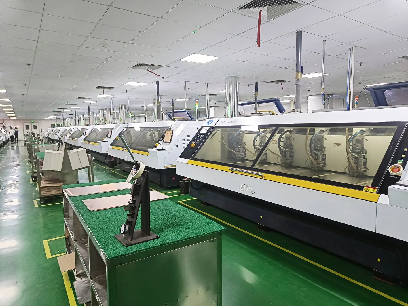
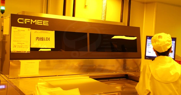
Advanced Manufacturing Techniques
- Laser Direct Imaging (LDI): Achieves trace widths as narrow as 15µm for intricate routing.
- Sequential Lamination: Builds layer stacks with precision, ensuring alignment across microvias.
- Via-in-Pad Technology: Flattened vias allow direct component mounting, saving space.
Quality Assurance
- Automated Optical Inspection (AOI): 3D scanners detect micro-defects like incomplete via fills.
- Cross-Sectional Testing: Validates plating uniformity and via reliability.
- Thermal Cycling: Exposes boards to -55°C to 150°C to test durability under extreme conditions.
PCB HDI in Action: Transforming Industries
From life-saving medical devices to cutting-edge AI hardware, PCB HDI is driving progress across sectors:
1. Consumer Electronics
- Smartphones: 12-layer HDI boards with embedded components for 5G antennas and foldable screens.
- AR/VR Headsets: Ultra-thin designs enabling lightweight, immersive experiences.
2. Medical Technology
- Implantable Devices: Biocompatible HDI boards for pacemakers and neurostimulators.
- Portable Diagnostics: Rugged, high-density boards for handheld ultrasound systems.
3. Automotive Innovation
- Autonomous Driving: HDI boards for LiDAR sensors and AI-powered ECUs (Electronic Control Units).
- EV Battery Management: Multi-layer designs with high-voltage isolation for safety.
4. Aerospace
- Satellite Communications: Radiation-hardened HDI boards with high-speed data links.
- Drones: Lightweight rigid-flex circuits for agile navigation systems.
Case Study
SprintPCB developed a 16-layer PCB HDI for a satellite communications startup, reducing signal latency by 45% while cutting board weight by 30%.
Overcoming PCB HDI Challenges
While HDI offers immense benefits, it requires expertise to navigate its complexities:
Thermal Management
- Challenge: High component density leads to heat buildup.
- Solution: Integrated thermal vias, copper coin inserts, and advanced heatsink materials.
Signal Integrity
- Challenge: Crosstalk in tightly packed traces.
- Solution: Ground shielding, differential pair routing, and impedance-controlled designs.
Manufacturing Precision
- Challenge: Microvia reliability in high-aspect-ratio designs.
- Solution: Laser parameter optimization and vacuum-assisted lamination.
SprintPCB’s team addresses these challenges through iterative prototyping and proprietary process controls, ensuring flawless production.
The Future of PCB HDI: Trends to Watch
As technology evolves, PCB HDI will continue to break new ground:
1. Embedded Components
Resistors, capacitors, and ICs integrated into inner layers, freeing surface space for critical components.
2. Additive Manufacturing
3D-printed circuits using conductive nano-inks for ultra-customizable geometries.
3. AI-Driven Design
Machine learning algorithms auto-optimize layouts for performance, cost, and manufacturability.
4. Quantum Computing
HDI boards with superconducting materials (e.g., niobium) for qubit control systems.
5. Sustainable HDI
Biodegradable substrates and lead-free solders to reduce environmental impact.
Why Partner with SprintPCB for PCB HDI?
- Technical Mastery: 15+ years of HDI manufacturing for Fortune 500 clients.
- Quick Turnaround: 48-hour prototyping for complex designs.
- Global Compliance: Certifications include IPC-6012 Class 3, IATF 16949, and ISO 13485.
- End-to-End Support: From design reviews to logistics, we streamline your journey.
Success Story
A leading automotive OEM leveraged SprintPCB’s PCB HDI expertise to develop an AI-driven ADAS module, achieving a 50% reduction in size while boosting processing power.