In the modern field of electronics, Printed Circuit Board (PCB) are indispensable key components. With the constant advancement of technology and evolving application needs, various specialized types of PCB have emerged, including Radio Frequency Printed Circuit Board (RF PCB). RF circuits play a vital role in communication, radar, satellite systems, and other domains, and RF PCB has become the preferred choice for many high-frequency applications.
In this blog post, we will focus on comparing the differences and applications between Radio Frequency PCB and conventional Printed Circuit Board. We will introduce the basic concepts and structures of conventional PCB and RF PCB, and explore their distinctions in terms of material selection, design requirements, and manufacturing processes.
Additionally, we will showcase real-world application examples to demonstrate the usage scenarios of both conventional PCB and RF PCB in different fields, aiding readers in understanding their respective advantages and suitability.
Whether you are an electronics engineer, a student, or simply someone interested in the field of electronics, this article will provide you with comprehensive insights into Radio Frequency PCB and conventional Printed Circuit Board.
We believe that through in-depth comparison and analysis of these two PCB types, you will be able to make better choices for your project requirements and achieve more efficient and stable electronic system designs. Now, let's delve into the fascinating differences and applications between Radio Frequency Printed Circuit Boards and conventional PCB!
What is a conventional Printed Circuit Board (PCB)?
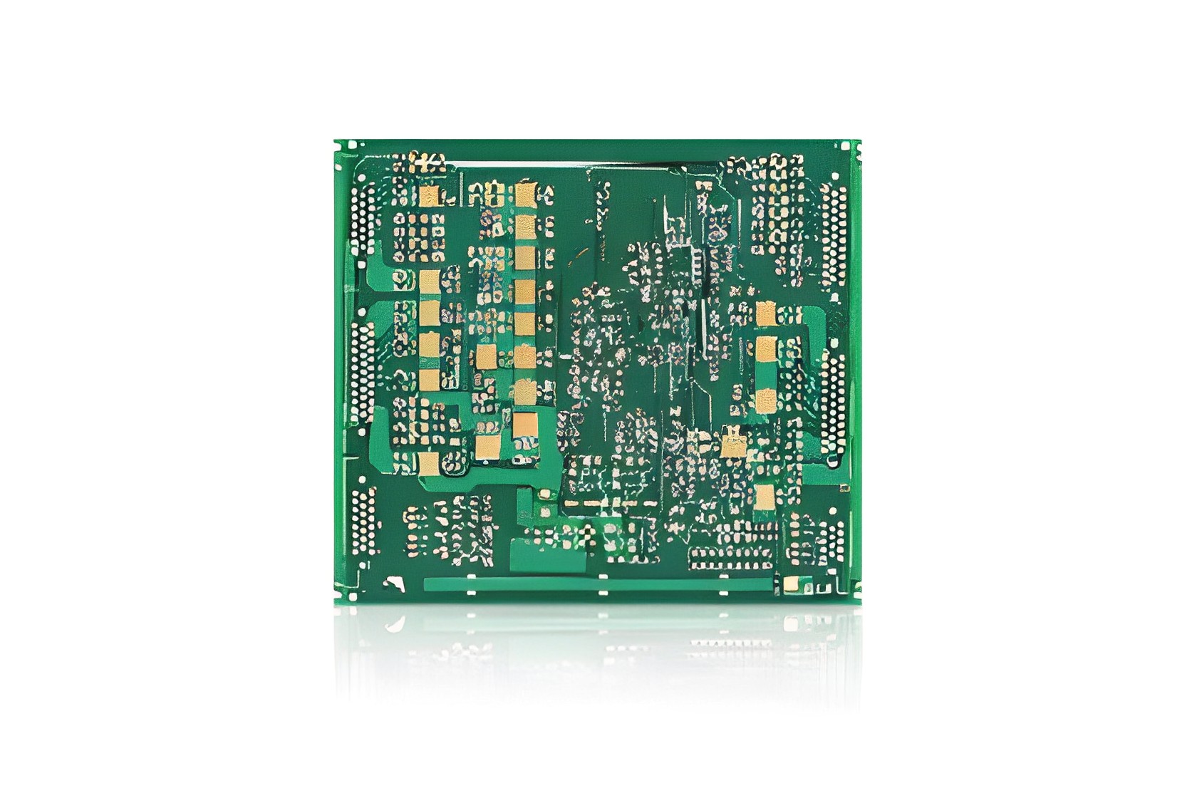
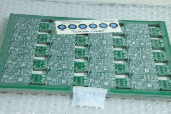
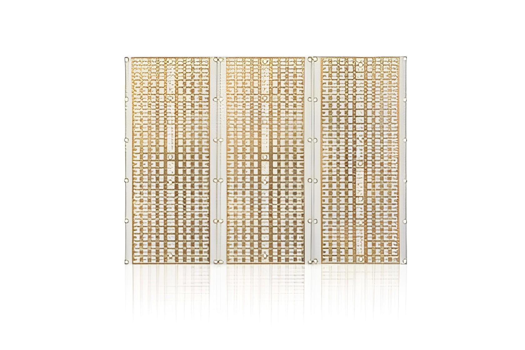
A conventional Printed Circuit Board (PCB) is a fundamental component used to support and interconnect electronic components. It is typically made of a non-conductive material, often referred to as FR-4, which is a fiberglass-reinforced epoxy laminate, with a layer or multiple layers of conductive material, typically copper, forming circuit paths on top of it.
The primary function of a PCB is to provide mechanical support and electrical connections by mounting electronic components, such as integrated circuits, resistors, capacitors, etc., on its surface and interconnecting them using copper traces. This design reduces circuit complexity while improving the reliability and stability of the circuit.
Conventional PCBs have the following characteristics and application areas:
Structure: Conventional PCBs feature a layered planar structure with copper traces interconnected through vias. They can be single-sided, double-sided, or multi-layered.
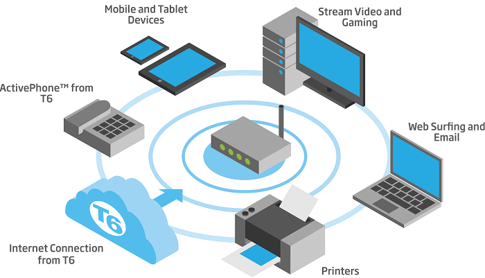
Applications: Conventional PCBs find wide-ranging applications in various electronic devices and products, including consumer electronics, communication equipment, industrial control systems, computer hardware, etc.
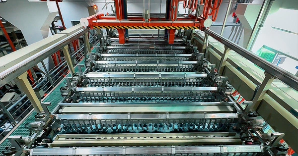
Manufacturing: Conventional PCBs are typically manufactured through processes involving printing and etching, where the conductive patterns are printed on the non-conductive substrate and unwanted copper material is chemically removed.
Features: Conventional PCBs are simple and cost-effective, suitable for general circuit designs and applications within a moderate frequency range.
Materials: Conventional PCBs predominantly use FR-4 as the substrate material, which offers good insulation properties and mechanical strength.
A conventional PCB is a versatile circuit board applicable to a wide range of electronic devices and applications. They possess a relatively simple structure and manufacturing process, making them cost-effective for general circuit designs.
What is a Radio Frequency Printed Circuit Board (RF PCB)?
A Radio Frequency Printed Circuit Board (RF PCB) is a specialized type of printed circuit board designed to handle high-frequency and radio frequency signals. In comparison to conventional printed circuit board (PCB), RF PCB has unique characteristics and design requirements that enable effective signal transmission within the high-frequency range.
Firstly, the design objective of an RF PCB is to achieve low loss and high-performance RF signal transmission. To accomplish this, RF PCBs need to consider impedance matching and signal integrity. Impedance matching is crucial in minimizing signal reflection and loss during signal transmission. Signal integrity refers to maintaining signal stability and accuracy throughout the transmission process, free from interference or attenuation.
Secondly, RF PCBs require the use of special materials and layer stack-ups to meet the demands of high-frequency signals. Common materials used for RF PCBs include PTFE (Polytetrafluoroethylene) substrates such as Teflon and Rogers. These materials exhibit low dielectric loss and high thermal stability, providing superior performance in high-frequency environments.
Moreover, RF PCBs necessitate precise and careful layout and routing. High-frequency signals impose stricter requirements on circuit layout and routing to avoid signal crosstalk and electromagnetic radiation. Therefore, RF PCBs often employ techniques such as layer partitioning, grounding planes, and differential transmission lines to minimize signal interference and noise.
Radio Frequency Printed Circuit Boards play a vital role in various application areas, including wireless communication devices (such as mobile phones and wireless routers), radar systems, satellite communication, and radio frequency spectrum analyzers. These applications demand precise transmission and reliability of high-frequency signals, and RF PCBs deliver the required performance and reliability.
A Radio Frequency Printed Circuit Board is specifically designed to handle high-frequency and radio frequency signals. It addresses the requirements of impedance matching, signal integrity, special materials, and precise layout to meet the demands of high-frequency environments. RF PCBs play a critical role in wireless communication, radar systems, satellite communication, and other fields, providing reliable performance for high-frequency signal transmission.
Differences between radio frequency PCB and conventional PCB:
There are significant differences in material selection between conventional printed circuit board (PCB) and radio frequency printed circuit board (RF PCB). These material choices play a crucial role in circuit performance and frequency response.
In conventional PCBs, commonly used base materials include glass fiber-reinforced epoxy resin (FR-4) and polyimide (PI). FR-4 is a widely used standard material with lower cost and good mechanical strength, suitable for most conventional circuit applications. Polyimide, on the other hand, offers higher temperature tolerance and better dimensional stability, making it suitable for applications with specific environmental requirements, such as high temperature or high humidity environments.
In contrast, material selection for RF PCBs is more refined and complex. Given the higher frequencies and stricter requirements of RF signals, choosing appropriate materials is essential for achieving optimal RF performance. Common RF PCB materials include polytetrafluoroethylene (PTFE), polyimide (PI), and low dielectric constant materials.
Polytetrafluoroethylene (PTFE) is a high-performance RF material with low loss, high frequency response, and excellent dielectric properties. It is widely used in high-frequency applications such as RF transmission lines, antennas, and filters. Using PTFE materials in RF PCBs helps reduce signal loss and improve the reliability of signal transmission.
Polyimide (PI) is also a common material choice in the RF field. It has low dielectric constant and dielectric loss, making it suitable for high-frequency and broadband applications. Using polyimide materials in RF PCBs enables better signal integrity and lower interference.
In addition to PTFE and PI, there are specially designed low dielectric constant materials for RF applications, such as low dielectric constant polyimide (LCP). These materials offer extremely low dielectric constant and loss, making them suitable for high-frequency RF applications, providing higher signal speed and better signal integrity.
Different designs in radio frequency PCB and PCB
Here are significant differences in the design requirements between conventional printed circuit boards and
radio frequency printed circuit boards.
RF signal transmission is critical for RF PCBs. Due to the high-frequency nature of RF signals, the design of RF PCBs needs to consider signal transmission and propagation. This involves careful routing and circuit layout to minimize signal loss and interference.
Conventional PCBs typically do not require specific attention to high-frequency signal transmission. They offer more flexibility in routing and layout. Conventional PCBs primarily focus on low-frequency signals and power transmission.
Strict impedance matching is essential for efficient and accurate RF signal transmission. RF PCBs have more stringent impedance control requirements, necessitating precise matching of impedance between signal sources, transmission lines, and loads.
Conventional PCBs have looser impedance control requirements and can tolerate certain impedance variations. The design of conventional PCBs emphasizes circuit functionality and connectivity rather than precise impedance matching.
RF signal transmission imposes higher demands on signal integrity. RF PCBs need to consider factors such as signal propagation delay, crosstalk, and power attenuation. Therefore, special routing techniques, circuit isolation, and shielding methods are employed in RF PCB design to maintain signal integrity.
Conventional PCBs have lower requirements for signal integrity. Conventional PCB designs prioritize circuit connectivity and reliable signal transmission, without excessive consideration for signal integrity concerns.
In summary, RF PCBs have more stringent design requirements, necessitating higher precision and expertise. Designers must have in-depth knowledge of RF circuits and high-frequency characteristics, employing specialized design techniques and process controls to meet the requirements of RF signal transmission.
On the other hand, conventional PCB design offers more freedom, focusing on circuit functionality and connectivity, with lower demands on high-frequency characteristics. Therefore, the choice between conventional PCBs and RF PCBs should be based on specific application requirements.
Different manufacturing processes for radio frequency PCB and PCB
The manufacturing process is another significant difference between conventional printed circuit board and radio frequency printed circuit board.
Manufacturing Process for PCBs:
Design and Layout: Using electronic design automation (EDA) software, the circuit design is translated into the PCB layout. This includes component placement and determining the routing paths of the PCB.
Substrate Creation: Conventional PCBs typically use a substrate material called fiberglass-reinforced epoxy resin (FR-4). The substrate is coated with copper foil, and unwanted copper is then removed using photolithography and chemical etching, forming the metal traces of the circuit.
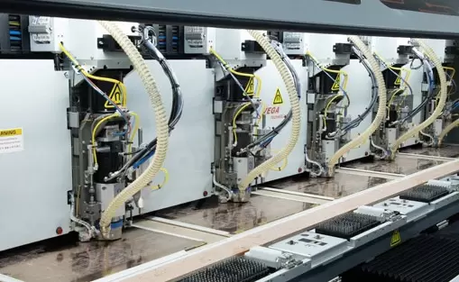
Drilling: Holes are drilled on the PCB for component installation and interconnecting the circuit.
Plating: A conductive material, usually copper, is coated onto the walls of the drilled holes to enhance connectivity.
Soldering: Electronic components are soldered onto the PCB. This can be done manually or using automated equipment such as wave soldering machines or reflow ovens.
Testing and Quality Control: Assembled PCBs undergo testing to ensure correct functionality and quality.
Manufacturing Process for RF PCBs:
Material Selection: RF PCBs often require specialized materials such as polytetrafluoroethylene (PTFE) or polyphenylene oxide (PPO) to meet the requirements of high-frequency signal transmission.
Specialized Lamination Process: RF PCBs may involve multilayer designs with different dielectric layers and metal layers. The insulation properties between these layers are crucial for RF signal transmission.
High-Precision Processing: Due to the unique nature of RF signals, RF PCBs require higher precision in processing, such as smaller drill diameters and more precise trace widths.
Impedance Control: RF PCBs need to strictly control signal impedance to ensure stable and consistent signal transmission. This may involve special design and manufacturing techniques such as microstrip or coplanar waveguide structures.
Stringent Quality Control: The manufacturing process of RF PCBs requires stricter quality control to ensure the circuit's performance meets the design requirements. This includes using high-precision testing equipment for signal and impedance measurements.
Application Examples: Conventional PCB and RF PCB in Real-World Applications
Application examples of Conventional PCB:
Consumer Electronics: Conventional PCBs are widely used in consumer electronic devices such as smartphones, tablets, personal computers, etc. They are used to connect and support various electronic components and functional modules, including processors, memory, sensors, etc. Conventional PCBs provide stable circuit connections and signal transmission in these devices.
Automotive Electronics: Electronic systems in automobiles require reliable circuit boards to support various functionalities, such as engine control units, infotainment systems, navigation systems, etc. Conventional PCBs are extensively used in automotive electronics to provide reliable signal transmission and power distribution.
Industrial Automation: In the field of industrial automation, conventional PCBs are used for the interconnection and interaction of control systems, sensors, and actuators. They play a critical role in production lines, robot control, and monitoring systems.
Application examples of RF PCB:
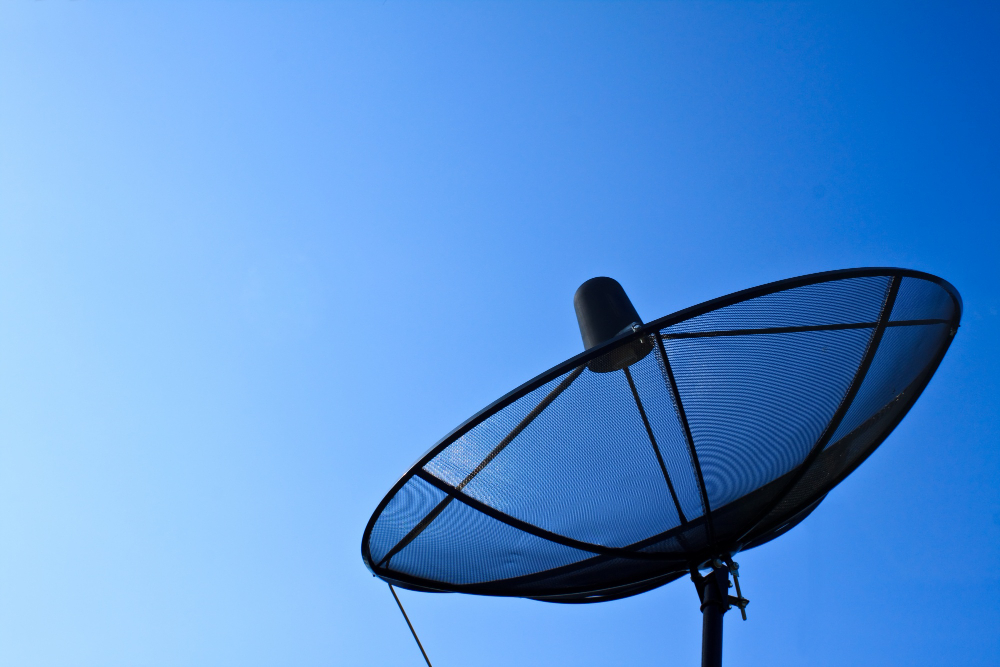
Wireless Communication: RF PCBs are crucial in wireless communication devices. For example, base station antennas, satellite communication equipment, wireless local area network (Wi-Fi) routers, etc., all require RF PCBs to achieve high-frequency signal transmission and impedance matching.
Radar Systems: Radar systems require high-frequency and high-performance circuit boards for precise signal processing and RF energy transmission. RF PCBs are widely used in civilian radar systems, such as weather radars, aircraft navigation radars, etc.
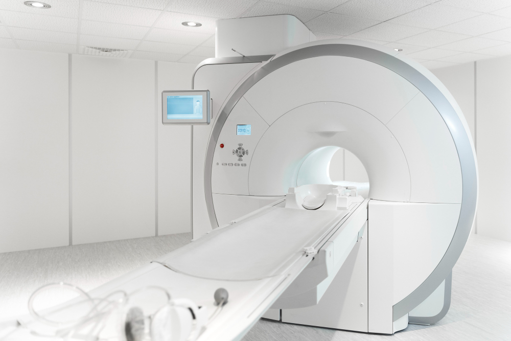
Medical Devices: Some medical devices, such as MRI scanners, pacemakers, and wireless medical sensors, require RF PCBs to achieve high-frequency signal transmission and accurate data processing.
In this article, we have extensively discussed the differences and applications between Radio Frequency Printed Circuit Boards (RF PCBs) and conventional Printed Circuit Boards (PCBs). We have found significant variations between these two types of circuit boards in terms of material selection, design requirements, and manufacturing processes.
In practical applications, conventional PCBs are widely utilized in general electronic devices, consumer goods, and industrial control fields. On the other hand, RF PCBs excel in domains such as communication, radar, radio frequency identification (RFID), and wireless sensor networks, where high-frequency performance is crucial.
Therefore, we strongly encourage carefully evaluating and comparing these two types of circuit boards based on specific requirements when selecting a suitable option. The choice should be made considering factors such as frequency demands, signal transmission characteristics, and performance requirements, ensuring optimal circuit performance and operational stability.
Lastly, if you are interested in learning more about these two types of circuit boards, please feel free to contact us.
Experience Top-Notch PCB Support with
SprintPCBCount on
SprintPCB, the leading high-tech enterprise, for all your PCB manufacturing needs. Our one-stop services cater to clients worldwide, ensuring a hassle-free process at competitive prices. Streamline your operations and reach out to us now to explore the myriad ways in which we can support your organization.