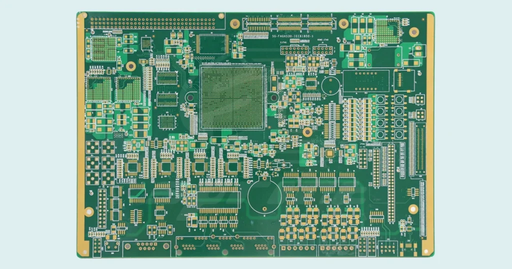
In this blog post, we will explore the challenges and solutions associated with Radio Frequency Printed Circuit Boards (RF PCBs). RF PCBs are a type of circuit board widely used in high-frequency signal transmission and RF electronic devices. With the rapid advancement of communication and electronic technologies, the design and manufacturing of RF circuits have become increasingly complex and critical. Therefore, understanding the challenges faced by RF PCBs and implementing appropriate solutions is essential to ensure high performance and reliability. To begin, let us first define RF PCBs and discuss their applications. RF PCBs are special types of circuit boards used for processing and transmitting high-frequency signals. They are commonly employed in wireless communication systems, radar, satellite communication, high-frequency filters, and other RF electronic devices. Due to the sensitivity of high-frequency signals to signal integrity and interference, careful attention is required in the design and manufacturing of RF PCBs. However, RF PCBs face several challenges during the design and manufacturing process. Primarily are the requirements for high-frequency signal transmission. High-frequency characteristics and signal integrity are critical considerations in RF circuit design. In the high-frequency range, signal transmission and reception become more challenging as the length and shape of signal paths significantly impact transmission characteristics. Moreover, signal interference and noise pose significant problems in high-frequency environments. Secondly, material selection and design optimization present challenges for RF PCBs. The performance of RF PCBs depends on the dielectric constant and loss factors of the substrate materials used. Proper material selection and design optimization can minimize signal loss and interference. Additionally, the design of transmission lines and antennas is crucial in RF PCBs, as they play a key role in signal radiation and reception. Thirdly, manufacturing processes also pose challenges. The manufacturing of RF PCBs requires careful consideration of circuit board layout and layer stacking to ensure optimal signal transmission performance. Furthermore, the application of grounding and shielding techniques is essential for reducing signal interference and electromagnetic radiation. Tolerance control and process requirements also need to be carefully considered to ensure the accuracy and stability of the manufacturing process. To address these challenges, several solutions have been proposed and widely implemented. During the design phase, high-performance materials can be used, and signal paths and layouts can be optimized to maximize the quality of signal transmission. Additionally, the application of simulation and analysis tools assists engineers in predicting and optimizing the performance of RF PCBs. In the manufacturing process, precise layer stacking and interlayer connections, along with advanced manufacturing techniques, can ensure the quality and performance of RF PCBs. Furthermore, stringent quality control and testing are crucial for ensuring the stability and reliability of RF PCBs. Testing and validation also play a significant role in ensuring the performance of RF PCBs. High-frequency measurements and characteristics analysis can help verify the quality and properties of signal transmission. Signal integrity and performance validation are critical steps in ensuring that RF PCBs adhere to design specifications. Lastly, continuous improvement and innovation are essential for the development of RF PCB technology. Keeping track of emerging technologies and industry trends and adopting them is crucial for maintaining a competitive edge. Simultaneously, continually improving the design and manufacturing processes to enhance the performance and reliability of RF PCBs is key to sustained development. In the following sections of this article, we will delve deeper into these solutions and showcase the practical applications and achievements of RF PCB technology through a successful case study. By understanding the challenges of RF PCBs and implementing the corresponding solutions, we can better meet the requirements of high-frequency signal transmission and drive the advancement of RF electronic devices.
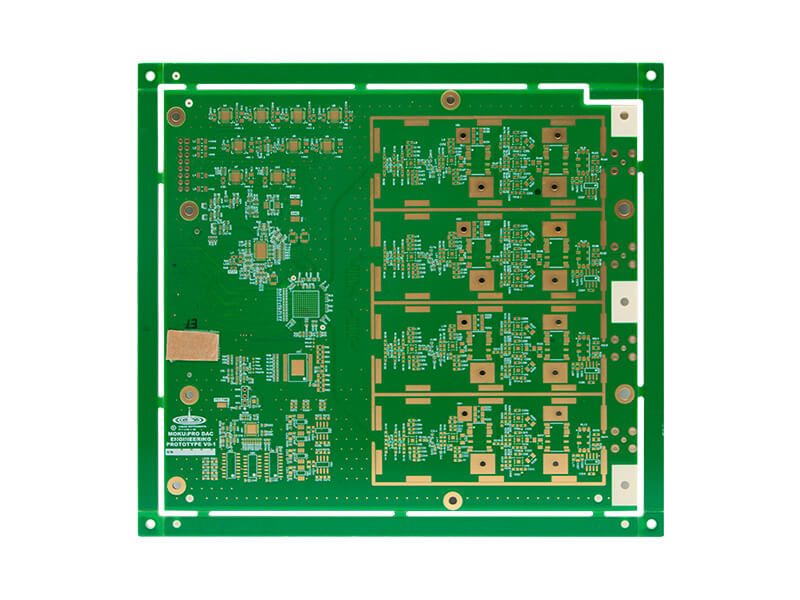
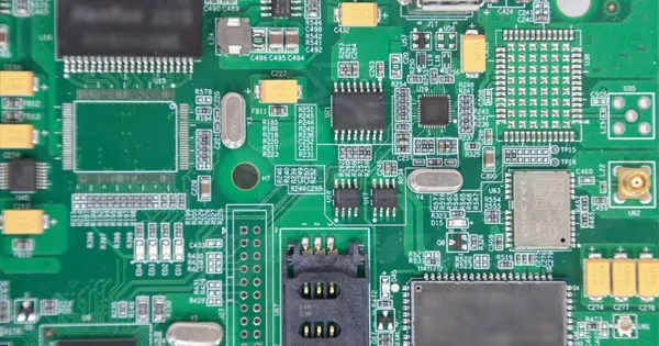
PCB Layout and Layer Stacking: the layout and layer stacking design of RF printed circuit boards need to consider signal integrity and electromagnetic compatibility. Proper PCB layout and layer stacking can reduce signal interference and crosstalk, improving RF performance.
Grounding and Shielding Techniques: effective grounding and shielding techniques are necessary in RF printed circuit boards to suppress interference sources and electromagnetic radiation. This includes proper grounding planning, ground plane design, and optimization of shielding structures.
Tolerance Control and Process Requirements: RF printed circuit boards have stringent tolerance control and process requirements during manufacturing. Precise control of dimensions, alignment, metallization, and soldering processes is crucial to maintaining RF performance.

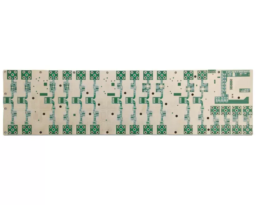
Case Study: Design and Manufacturing of RF PCB for 5G Base StationsBackgroundWith the rapid development of 5G communication technology, higher demands are placed on RF PCBs. A communication equipment manufacturing company decided to develop a high-performance base station based on 5G technology. To meet the requirements of high-frequency signal transmission, signal integrity, and performance stability, they chose RF PCBs as a critical component for the base station.SolutionConsiderations during the design phase: During the design phase, advanced RF circuit design tools and simulation software were utilized to optimize signal paths, ensuring the best signal integrity and transmission performance. Additionally, special materials with low dielectric constant and low loss were selected to minimize signal attenuation and transmission loss. Technical solutions during the manufacturing process: To ensure the quality and performance of the RF PCB, precise layer stacking and interconnection techniques were employed. By optimizing the PCB layout and implementing shielding techniques, signal interference and noise were significantly reduced. Advanced microfine circuit pattern fabrication processes and high-precision control were employed to ensure accurate dimensions and tolerance control. Testing and validation: Comprehensive high-frequency measurements and characteristic analyses were conducted to ensure that the RF PCB met stable performance within the design frequency range. Professional signal integrity analysis tools were used to verify the signal transmission and interface reliability of the PCB. Achievements and Benefits High performance and stability: Through the adoption of optimized design and manufacturing solutions, the RF PCB for the 5G base station achieved the requirements for high-frequency signal transmission, demonstrating excellent signal integrity and stability. Performance enhancement and market competitiveness: The successful launch of the high-performance base station based on 5G technology enhanced customer satisfaction and strengthened the company's competitiveness in the communication equipment market. The improved reliability and stability of the RF PCB contributed to the product's performance enhancement. Technological accumulation and innovation: Throughout this project, the company's design and manufacturing teams accumulated valuable experience and knowledge regarding RF PCBs. This provides a solid technical foundation and supports future projects with continued innovation. This successful case study exemplifies the importance and application value of RF PCBs in fields such as 5G communication. Through proper design and manufacturing solutions, RF PCBs can meet the requirements for high-frequency signal transmission, providing stable performance and reliability, thereby driving the advancement of modern communication technology. In this article, we have discussed the challenges faced in the design and manufacturing of Radio Frequency Printed Circuit Boards (RF PCBs) and proposed solutions to overcome them. RF PCBs play a critical role in modern communication and electronics, but the high-frequency signal transmission requirements, material selection, and manufacturing complexities pose challenges. However, by implementing appropriate solutions, we can ensure the performance and reliability of RF PCBs. During the design phase, considerations such as using high-performance materials, optimizing signal paths and layouts, and employing simulation and analysis tools help evaluate design options. Technological solutions in the manufacturing process include precise layer stacking and interconnects, advanced manufacturing processes, and stringent quality control and testing. The testing and validation phase involves techniques like high-frequency measurements, performance analysis, and signal integrity verification. Continual improvement and innovation are key factors in the success of RF PCBs. Tracking emerging technologies and industry trends and continuously improving design and manufacturing processes enhance the performance and reliability of RF PCBs. Through successful case studies, we observe practical applications and achievements resulting from these solutions. These cases provide insights into the design and manufacturing process of RF PCBs and offer guidance for future projects. In conclusion, RF PCBs play a crucial role in modern communication and electronics, but they face challenges during the design and manufacturing phases. However, with appropriate solutions, these challenges can be overcome to ensure the performance and reliability of RF PCBs. As technology continues to advance, we can expect RF PCBs to play an even more significant role in future improvements and innovations.

Customer support