The utilization of a high-quality solder mask is crucial in the manufacturing process of printed circuit boards. If a PCB lacks a reliable Soldermask, its durability will be significantly reduced. Creating an effective solder mask involves several factors and is a critical component of your PCB's composition.
What is a Solder Mask?
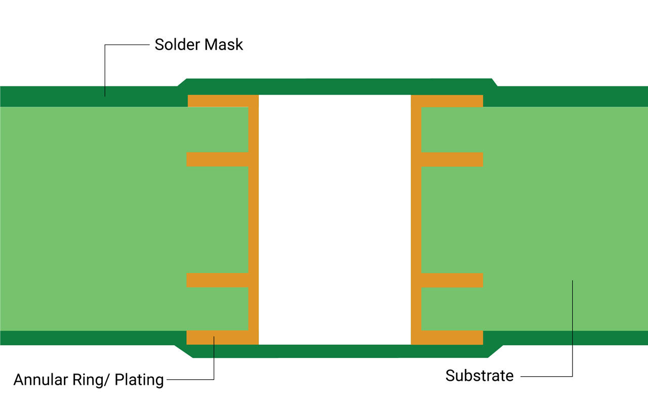
Soldermask is a liquid photoimageable lacquer used to safeguard the copper on the circuit board by providing a protective layer. It is applied to both sides of the PCB to shield the copper from various issues that could cause malfunction, such as oxidation, external conductive influences, soldering, high voltage spikes, environmental elements, and others.
Types of soldermask
PCBs have different types of Solder mask.Regardless of the type, they all undergo a thermosetting process after the pattern is determined.The types of Soldermask are shown below:
Epoxy Liquid
solder mask comes in different media depending upon the demands of the application. The lowest-cost Soldermask is epoxy liquid that is silkscreened through the pattern onto the PCB.
LPSM(liquid photoimageable Soldermask)
LPSM can be silkscreened or sprayed on the PCB, exposed to the pattern and developed to provide openings in the pattern for parts to be soldered to the copper pads.
DFSM(dry film photoimageable Soldermask)
DFSM is vacuum laminated on the PCB then exposed and developed.
During the printed circuit board fabrication process, the solder mask is sprayed onto the production panel, and then UV exposure is applied with the appropriate solder mask pattern. Subsequently, the mask is developed and dried. Although green is a common color for soldermask on PCBs, it is also available in other colors, and clear solder mask is also an option.
Defining Soldermask Layers in Gerber Data
When working with Gerber data, it is important to understand how to define soldermask layers. soldermask layers in Gerber data should be considered as a negative image. This means that where you see color on the mask layer, there should be no solder mask coverage. Everywhere else on the board will be covered with soldermask. Think of the solder mask as completely covering your PCB board, and the soldermask files indicate the areas where no solder mask should be applied.
In the Gerber data for rigid boards, GTS represents the Top Soldermask layer, while GBS represents the Bottom Soldermask layer. For flex or rigid-flex PCBs, both GTS and GBS can be used for soldermask and coverlay layers.
During the process of issuing Gerber files (CAM engineering), SprintPCB will automatically adjust the soldermask apertures as needed for PCB production. Typically, a soldermask aperture is adjusted to be 4 mil larger than the copper pad it is exposing (2 mil larger on each side). This adjustment ensures that the mask is centered on the pad and avoids any solder mask covering the copper pad. The tolerance for soldermask registration is typically +/-2 mil, which is why apertures are adjusted to be 2 mil larger all around the copper feature, ensuring the entire pad can be soldered.
There are situations where a soldermask defined (SMD) pad is required. A SMD pad is when the soldermask relief is the same size or smaller than the copper pad it is exposing. These pads are commonly used when soldermask dams are needed between surface mount device pads, but there is not enough space to print a dam and follow the standard soldermask swell. If you require a soldermask defined pad and do not want soldermask clearances to be modified, it is important to include a fabrication note stating which pads should not be adjusted.
How to Apply LPI Soldermask on Printed Boards?
LPI solder mask can be applied to a PCB through a silkscreening process. It is then exposed to the desired pattern and developed, creating window openings in the pattern for components to be soldered onto the copper pads. On the other hand, Dry Film Solder Mask (DFSM) is vacuum-laminated onto the PCB and then exposed and developed. Both processes typically undergo a thermal cure to finalize the pattern. However, LPI soldermasks are also available in ultra-violet (UV) cure variants.
In the past, soldermasks were commonly applied using dry film sheets. However, with the advancements in LPI solder masks and related techniques, DFSM is rarely used today. SprintPCB primarily utilizes LPI (Liquid Photo Imageable) solder masks, which have become the prevailing choice. LPI masks offer enhanced reliability, precise printing capabilities, and improved contact with the board's surface and copper features, providing superior protection. These solder masks are made from epoxy-based materials, making them exceptionally durable and almost impossible to remove once fully cured.
Here is a step-by-step process for applying LPI solder mask on printed boards:
- Thorough Cleaning: The PCB production panel undergoes a meticulous cleaning process to eliminate any dust particles or contaminants that may compromise the solder mask application. This step ensures a clean surface for optimal adhesion.
- Full Coverage: The panels are completely coated, either on a single side or both sides, with the LPI soldermask. This ensures comprehensive coverage of the board surface.
- Tack-Drying: The coated panels are then placed in an oven for tack-drying. This process partially cures the soldermask, allowing it to reach a sticky state that facilitates further processing.
- Film Preparation: A film is prepared based on the soldermask Gerber files, with separate films for each side of the board. The areas on the film that correspond to where the soldermask should adhere are clear, while the areas to be removed are represented as black.
- UV Exposure and Development: The tack-dried boards are inserted into a UV developer. The film is precisely aligned over the board, ensuring accurate placement. The blacked-out sections on the film prevent the UV light from curing the soldermask in those areas, enabling precise removal of unwanted mask material.
It is important to note that LPI solder masks offer exceptional reliability and durability, making them a preferred choice in modern PCB manufacturing.
Solder Mask VS. Paste Mask
Solder masks and paste masks are often mentioned in the same setting, making it challenging for beginners to draw a line between them.
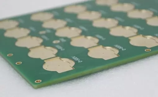
If you've ever seen a PCB, you're undoubtedly familiar with its predominantly green coloring. This thin green protective coat on the top and bottom surfaces of a board is the soldermask. Despite their importance, solder masks aren't a critical necessity for all PCBs.
There can also be circumstances where you want a mask on the top but not the bottom layer, or vice versa. Solder mask essentially covers the entire top or bottom surface, only leaving out the areas where components would make circuit board shopping; various things might get you confused. Whether you are going for a single-sided PCB, a double-sided PCB, or any other type of PCB, You can contact the board's copper traces.
Paste mask, on the other hand, is a material that is applied to the areas that have been left uncovered by the soldermask to assist in the soldering process.
The paste is commonly used to connect surface-mount components to pads on a PCB during soldering. Still, it is can also work with through-hole pin-in-paste details by using a stencil, a syringe, or jet printing to apply the mask in or over the holes.
The solder paste's adhesive properties enable it to stick a component in place, after which the board is heated, melting the mask and creating both an electrical as well as a mechanical bond between the part and the surface.
So, while solder mask is used, during manufacturing, to prevent the oxidation of copper traces and the formation of solder bridges, paste mask is applied, during assembly, onto the points where component pins make contact with the PCB to facilitate a firm, reliable bond between them.
Stencils made for soldermask application are different from those made for paste masks in that the former leaves uncovered the areas on a board that the latter covers, and vice versa.
The paste mask is typically gray, but as you can learn in the next chapter, a solder mask is available in many colors.
Soldermask Colors
Although the solder mask has been exclusively green for a while, more shades are emerging to cater to designs with specific color requirements. To make prototype runs and revision changes more identifiable, merely make a PCB look trendy in a see-through enclosure.
With OEMs increasingly embracing clear electronics and appliances, circuit board manufacturers are adopting colored soldermasks as a way to give their boards a bit of a personality.
Commonly Used Solder Mask Colors
Today, the most widely used colors are red, blue, black, white, and yellow. Clear – not technically a color – is also a shade of choice for designers. And manufacturers can also synthesize other decisions, such as purple, orange, or even pink, from the three primary colors – red, blue, and yellow.
Green
Although the color spectrum for solder masks has expanded significantly in recent years, most PCBs still come covered in the green mask. One of the primary reasons why green is the preferred color for many designers is that it aids in the inspection.
According to research, the eyes are more sensitive to green than colors like yellow, white, or black, making it easier to see the contrast between copper pads, traces, and empty spaces.
Additionally, the green mask adheres relatively evenly, cures appropriately, and has a higher resolution than most colors. This means it can create smaller mask dams for a more space-efficient circuit.RedDesigners, especially those in modern niches like Artificial Intelligence and the Internet of Things, increasingly embrace red soldermasks for aesthetic purposes. In some circuits, red can also give a more striking color contrast between a board's components and traces and silkscreen.
Blue
Blue and green soldermask are very similar in functionality, but for some PCB users, blue takes the win because of its uniqueness. Boards covered in the blue front are pretty rare on the market. But if you want them for your project, you can get them from a manufacturer like SprintPCB.
Black
While not exactly the most eye-catching, Black soldermask can be advantageous in applications that require light reflection. Also absorbs heat more readily than other colors, and that means it needs less heat during reflow.
White
White is the most unpopular PCB solder mask color because it provides the most negligible visibility. Moreover, some low-quality masks start to turn yellow after a while, especially when consistently exposed to heat.
Nevertheless, white masks are often the first choice for LED systems because they're brighter than other PCB colors.
Other Colors
If none of the shades above float your board, you can consider rarer but more uniquely appealing solder mask colors like yellow, orange, and purple. These colors are popular among companies that make niche electronics and designers looking to make their new products stand out in the market.
If you want an exceedingly compact circuit, a transparent mask will give you the most miniature mask dams and mask reliefs compared to other colors.
Choosing The Right Color
Although experimenting with different shades can make your project look a lot more interesting than with the standard green, it pays to know that the color you choose will, to some extent, impact the performance of your solder mask.
For starters, black, white, and yellow are known for their poor resolution because UV light doesn't always penetrate the entire coating. A PCB masked with these colors will have fewer tracks than a similarly-sized board with a green, red or blue mask.
On the flip side, although transparent soldermasks give the highest resolution, they're susceptible to color shifts during the many thermal excursions and chemical treatments a PCB encounters.
The performance of a color type is also determined by the quality of the solder mask itself. Top suppliers usually have custom shades that provide high resolution, as well as temperature and chemical resistance.
Designers often use different-colored solder masks for mere aesthetics. Still, if you don't have specific color considerations, various shades can help you identify your boards during assembly and beyond.
You can use red, blue, and black to mark different prototype stages of the design and then settle on green or white for the final product.
How to Measure Soldermask Thickness?
While a sufficient thickness of solder mask is necessary to safeguard the circuits, it's crucial to measure the solder mask's thickness to ensure it's not excessive. For the conductor's top and side edges, a thickness greater than 7 microns is preferred. The maximum thickness for solder masks on finished copper parts up to 35 micrometers is 40 micrometers, while for thicker copper, it can be up to 80 micrometers.
To ensure the effectiveness of the soldermask, it's recommended to follow the following guidelines:
- Meet the minimum annular ring requirements if the solder resist comes into contact with the lands.
- Avoid leaving exposed isolated pads.
- Allow solder resist only on plated through holes that are not intended for solder fill.
- Avoid applying solder resist on test points or connector fingers.
Achieving the appropriate thickness when applying soldermask is a delicate process and is one of many challenges that manufacturers face when producing high-quality printed circuit boards. At Sprintpcb, we have extensive experience in all aspects of well-designed PCB manufacturing, and we are delighted to share our knowledge with you.
If you require more information on soldermask thickness requirements, methods for measuring solder mask thickness, or any other issues relating to the manufacturing, distribution, or quality assessment of printed circuit boards, we are here to assist you.
Contact Sprintpcb today to speak with one of our skilled PCB professionals.
what we allow and what not
- The Soldermask may encroach on lands as long as the minimum annular ring requirements are maintained.
- Soldermask is permitted in those PTH not intended for solder fill.
- No isolated pads are exposed.
- No Soldermask encroachment on edge board connector fingers or test points.
- On SMT-pads with pitch 1,25 mm encroachment is permitted on one side of land only and does not exceed 50 micron (2 mil)
- On SMT-pad with pitch < 1,25 mm encroachment is permitted on one side of land only and does not exceed 25 micron (1 mil)
IPC-SM-840D | Qualification and Performance Specification of Permanent Solder mask This specification outlines the qualification and performance requirements for permanent soldermasks. It introduces two distinct classes, namely T and H, which represent different functional performance requirements and testing severity. The classification of a solder mask to a specific class should not be extended to cover any other class.
T - Telecommunication: This class encompasses various applications such as computers, telecommunication equipment, sophisticated business machines, instruments, and certain noncritical applications. Solder masks in this class are suitable for high-performance commercial and industrial products that require an extended performance life. Although interrupted service may occur, it is not life-threatening.
H - High Reliability: This class includes equipment where continuous performance is critical, where equipment downtime is unacceptable, and/or where the equipment serves as a life support item. Solder masks in this class are suitable for applications that require a high level of assurance and uninterrupted service is essential
.
Notes:
Class Designations: Previous versions of this IPC specification and other related specifications refer to "Class 1," "Class 2," and "Class 3" end product classes. However, for practical purposes, there is no Class 1 solder mask. The requirements outlined in this specification do not apply to solder masks used in Class 1 end products. Class 2 is equivalent to Class T (Telecommunications), while Class 3 is equivalent to Class H (High Reliability).