PCBs are essential components in electronic devices and are used to connect and provide power to various electronic components. Multilayer PCBs are used in more complex electronic devices such as computers, smartphones, and medical equipment. The manufacturing process of multilayer PCBs is more complex than that of single-layer PCBs and requires advanced technology and expertise. In this article, we will provide a simple guide to help you understand the manufacturing process of multilayer PCBs.
In this article, we will provide you with 10 simple guidance on the manufacturing process of multilayer PCBs, telling you the process and specific steps of making multilayer boards.
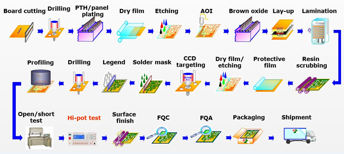
First of all, how many steps are there in the manufacturing process of multilayer PCBs? The answer is 10 steps, including design, inner layer production, drilling, chemical copper plating, lamination, pressing, outer layer graphic processing, outer layer chemical copper plating, hardening, and final processing. Next, I will give you a brief introduction to these 10 processes to help you quickly understand them.
Multilayer design
PCB manufacturers' design engineers use PCB design software for circuit diagram design and PCB layout design. The design engineer will choose suitable PCB design software, such as Altium Designer, Eagle PCB, etc., according to the needs. After selecting the PCB design software, the engineer will create a new PCB project in the software, set the board size, number of layers, materials, etc. Then, the engineer will draw the circuit diagram in the software, add components, connection lines, and set the attributes and values of the components. Finally, a netlist is generated for subsequent layout and wiring.
Next is the layout design phase, where components are arranged according to their connection relationships in the circuit diagram, and the position, orientation, spacing, etc. of each component are set. After layout is complete, wiring is carried out to connect the connection lines between components with wires or traces. After wiring is complete, silk screen, solder pads, and other markings and components are added. After completing these steps, a design rule check is performed to ensure that the layout and wiring comply with PCB manufacturing requirements and standards.
Finally, Gerber files are generated for PCB board manufacturing.When it comes to Gerber files, one might ask: What is a Gerber file?
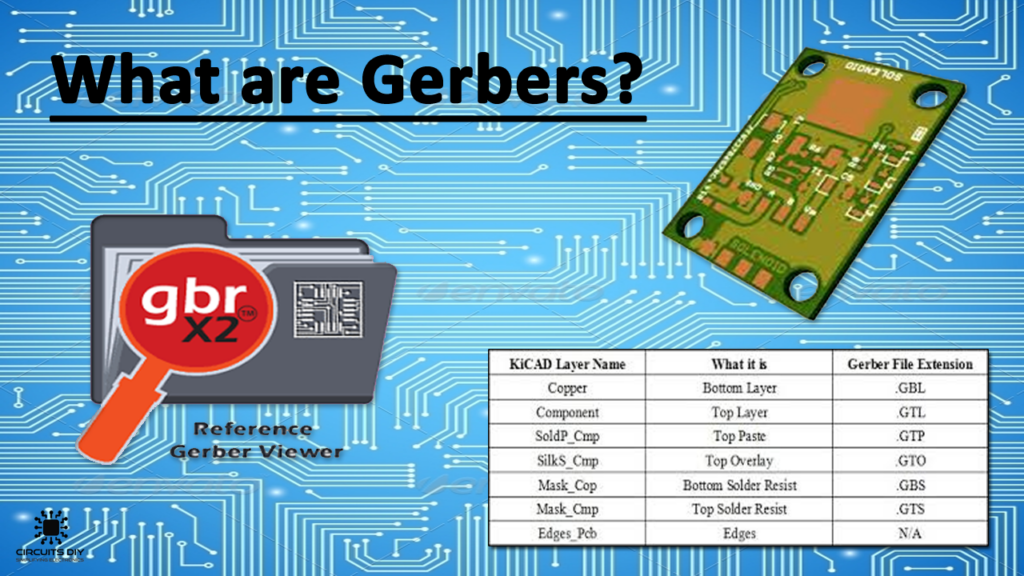
Gerber files are a standard file format used for manufacturing PCBs. They contain graphical information about various layers of the PCB, such as components, traces, pads, silkscreen, and more. Gerber files are typically generated by PCB design software and are used to convey the PCB's graphical information and manufacturing requirements to PCB manufacturers.
Gerber files consist of several files, including:
Top Layer: contains information about the components, traces, pads, and other features on the top layer of the PCB.
Bottom Layer: contains information about the components, traces, pads, and other features on the bottom layer of the PCB.
Silkscreen Layer: contains information about the silkscreen on the PCB, such as component names and locations.
Solder Mask Layer: contains information about the position and shape of solder pads on the PCB.
Drill File: contains information about the locations and sizes of holes that need to be drilled in the PCB.
Gerber files are an essential part of the PCB manufacturing process. They convert the circuit diagram designed by the PCB designer into graphical information that manufacturers can understand and use to produce the PCB. Manufacturers use Gerber files to produce PCBs and follow the requirements specified in the Gerber files during processing, drilling, copper etching, and other manufacturing processes.
Multilayer PCB inner layer production
First, the manufacturer needs to prepare materials such as glass fiber cloth, copper foil, pre-preg, and resin. Then, the surface of the glass fiber cloth is cleaned to ensure that the copper foil can firmly adhere to it. Next, a layer of pre-preg is applied to the surface of the glass fiber cloth, which can enhance the physical properties and durability of the glass fiber cloth. The glass fiber cloth coated with pre-preg is then placed in an oven to dry completely. After drying, the manufacturer places the copper foil on the pre-preg and uses a laminating machine to press them together. This step can make the copper foil tightly adhere to the pre-preg and form an inner layer board. Finally, the manufacturer uses a cutting machine to cut the inner layer board into the required size and shape for subsequent processing.
Multilayer drilling
First, the manufacturer selects appropriate drill bits and sets the diameter and depth of the drill bits according to the multilayer PCB design specifications. Drill bits are distinguished by different colors to match the machine. Next, the multilayer PCB is placed on the drilling machine and aligned with the positions that need to be drilled optically or mechanically. The drilling machine is used to drill holes, and the drilling speed and depth need to be set according to the multilayer PCB design specifications. During the drilling process, it is necessary to control the drilling depth to avoid damaging the inner layer board. After drilling, the PCB needs to be cleaned to remove debris and waste. The quality of the drilling needs to be inspected to ensure that the diameter and depth of all holes meet the multilayer PCB design specifications.
Multilayer chemical copper plating
The produced PCB board is cleaned to remove surface dirt and grease. Alkaline or acidic cleaning agents are usually used for cleaning. After cleaning, a layer of anticorrosive agent is coated on the surface of the PCB board to protect the non-conductive areas of the PCB board from being plated with copper. To facilitate the subsequent copper plating process, the manufacturer will coat a layer of catalyst on the surface of the PCB board. Then, the PCB board is placed in a chemical copper plating tank, and a layer of copper is plated on the surface of the PCB board through an electrochemical reaction. This process needs to control parameters such as temperature, current, and time to ensure the uniformity and quality of copper.
There are residues and impurities on the surface of the PCB board immediately after copper plating, which need to be cleaned and removed. Then, chemical substances are used to remove the anticorrosive agent and catalyst on the surface of the PCB board. Finally, the chemically plated PCB board is inspected to ensure that the thickness and uniformity of the copper meets the PCB design specifications.
Multilayer stacking
Before stacking, the prepared inner layers need to be cleaned and undergo corrosion protection to ensure the smoothness and cleanliness of the copper surface. The required prepreg layers should be prepared according to the PCB design specifications. Next, the stacking process involves assembling the prepared inner layers and prepreg layers according to the PCB design specifications.
Each layer needs to be pressed together using a laminating machine to ensure strong adhesion between the layers. After stacking, the multilayer board needs to be dried and drilled. It is placed in an oven for drying, and the drill holes are set according to the PCB design specifications. The multilayer board is then chemically plated with copper to enhance its conductivity and corrosion resistance. Finally, the edges of the multilayer board are subjected to edge trimming and surface treatment to remove unnecessary parts and ensure compliance with the PCB design specifications and subsequent printing and soldering processes.
Multilayer lamination
Prepare the inner layers, prepreg layers, and auxiliary materials such as press plates and spacers for lamination. Apply the prepreg layer onto the copper surface of the inner layers, ensuring an even coating. Stack the prepreg-coated inner layers together, placing spacers between each layer to maintain the desired distance and gap according to the PCB design specifications.
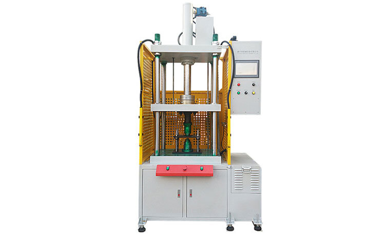
Place the stacked multilayer boards into the press plates and use a laminating machine for lamination. During the lamination process, it is necessary to control parameters such as pressure, temperature, and time to ensure strong adhesion between the layers. After lamination is completed, the multilayer boards are placed in a cooling chamber for cooling to ensure complete curing.
By the way, the laminating machine is one of the key equipment used in the manufacturing process of multilayer PCBs. Common types of laminating machines include flatbed laminators, rotary laminators, and hot presses, among others.
Outer layer patterning
Prepare the fiberglass substrate and cut it according to the PCB design specifications. Clean the substrate thoroughly. Next, apply a photosensitive resist onto the copper layer of the substrate, ensuring an even coating. The
multilayer PCB design pattern is then exposed onto the substrate using an exposure machine. The photosensitive resistance in the exposed areas undergoes a chemical reaction.
After exposure, the substrate is developed in a developer machine, which dissolves the unexposed photosensitive resist. Subsequently, the developed substrate is placed in a copper plating tank for copper plating, enhancing its conductivity and corrosion resistance. The copper-plated substrate still contains photosensitive resist in the unexposed areas, which needs to be removed by immersing it in a photosensitive resist stripping solution. Finally, the photosensitive resist-stripped substrate undergoes processes such as cutting and drilling to create the actual PCB board.
The outer layer patterning is an important step in the PCB manufacturing process, primarily used to transform the PCB design pattern into an actual PCB board. This process must be carried out in a controlled environment to ensure multilayer PCB board quality and precision. Any errors or improper operations can result in multilayer PCB manufacturing failures or decreased performance of the final electronic device.
outer layer chemical copper plating
Outer layer electroplating is an important step in the
multilayer PCB manufacturing process, primarily used to enhance the conductivity and corrosion resistance of the PCB. The PCB is placed in a cleaning tank for removing surface dirt, grease, and other impurities. After cleaning, the PCB is immersed in a chemical copper plating tank. In the chemical copper plating process, copper ions are electrolytically reduced onto the surface of the PCB, forming a uniform copper film.
The chemically copper-plated PCB is then placed in a cleaning tank to remove chemical agents and impurities from the surface. Subsequently, the chemically copper-plated PCB is immersed in a gold plating tank to improve its corrosion resistance and conductivity. Finally, the gold-plated PCB is cleaned in a cleaning tank to remove any remaining chemical agents and impurities from the surface.
Multilayer Curing
Multilayer PCB curing is an important step in the PCB manufacturing process, primarily used to enhance the mechanical strength and corrosion resistance of the PCB board. The curing agent is applied onto the surface of the PCB board, ensuring an even coating. The PCB board coated with the curing agent is then placed in an oven for drying to achieve surface dryness.
The dried PCB board is placed in a curing chamber for the curing process. In the curing chamber, the curing agent undergoes cross-linking reactions through methods such as heat reaction or UV irradiation, forming a hard and corrosion-resistant protective layer. After curing, the PCB board is removed from the curing chamber and placed in a well-ventilated area for cooling. The cured PCB board is inspected to ensure a uniform, smooth surface without any defects such as bubbles.
final processing
Multilayer PCB final processing is the last step in the PCB manufacturing process, primarily used to cut and drill the finished PCB boards to meet the actual requirements of electronic devices. The prepared PCB boards are placed into a cutting machine to be cut into various sizes and shapes as required. Subsequently, the cut PCB boards are loaded into a drilling machine for drilling holes of various sizes and shapes according to the PCB design specifications. Burr and residue around the drilled holes of the PCB boards need to be removed through a deburring process.
The deburred PCB boards are then cleaned in a cleaning tank to remove surface dirt, grease, and other impurities. Finally, the processed PCB boards are inspected to ensure their dimensions, shapes, and hole placements comply with the PCB design specifications. The inspected PCB boards are packaged for storage and transportation.
In this article, we have provided a detailed overview of the manufacturing process of multilayer PCBs, including PCB design, inner layer fabrication, multilayer lamination, drilling, outer layer processing, and other essential steps. These steps must be carried out in a controlled environment to ensure the quality and precision of the PCB boards.
Additionally, we have discussed other important steps such as outer layer electroplating, PCB curing, and PCB final processing. Through these steps, we can produce high-quality and high-performance multilayer PCBs that meet the requirements of various electronic devices. PCB manufacturing is a complex process that requires expertise and skills in various domains. If you need to manufacture high-quality PCB boards, we recommend choosing
SprintPCB as your manufacturing partner.
SprintPCB possesses advanced equipment and extensive experience to provide you with high-quality PCB manufacturing services.