The
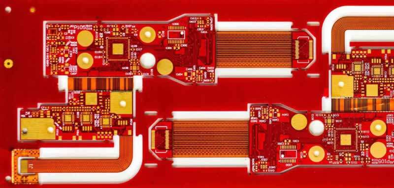
Rigid Flex PCB manufacturing process is a complex and meticulous series of steps that combine rigid and flexible circuit board technologies into a single, integrated product. This process ensures the creation of high-quality, reliable, and versatile PCBs suitable for a wide range of applications. Below is a detailed breakdown of the Rigid Flex PCB manufacturing process:
Design and Layout
Initial Design: Engineers begin with creating a detailed schematic and physical layout of the Rigid Flex PCB, specifying the rigid and flexible areas. This is done using advanced CAD software to ensure precision and efficiency.
Layer Stack-Up Planning: The stack-up is planned, defining the number and order of rigid and flexible layers. This step is crucial for determining the board’s mechanical and electrical properties.
Material Selection
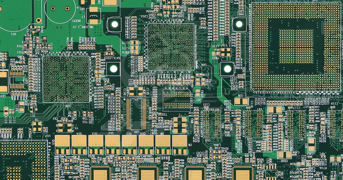
Substrate Selection: High-quality polyimide is chosen for the flexible layers due to its excellent thermal stability and dielectric properties. FR4 or similar materials are selected for the rigid sections.
Copper Cladding: Both the rigid and flexible substrates are clad with a thin layer of copper, which will form the circuit traces.
Imaging and Etching
Photoresist Application: A photoresist layer is applied to the copper-clad substrates. This light-sensitive material helps in creating the desired circuit patterns.
Exposure and Development: The photoresist is exposed to UV light through a photomask that defines the circuit design. The exposed areas are developed, washing away the unexposed photoresist.
Etching: The substrates undergo a chemical etching process that removes the exposed copper, leaving behind the circuit patterns.
Lamination
Prepreg Application: Prepreg (a partially cured resin material) is applied between the layers to bond them together.
Layer Alignment and Stacking: The rigid and flexible layers are precisely aligned and stacked in the correct order.
Heat and Pressure: The stack is subjected to heat and pressure in a lamination press, bonding the layers into a single cohesive structure.
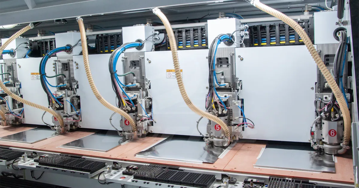
Drilling and Plating
Drilling: Precision drilling machines create holes for vias and through-holes, which provide electrical connections between the layers.
Hole Plating: The drilled holes are plated with copper to establish electrical connections, involving depositing a thin layer of copper inside the holes.
Pattern Plating and Etching
Pattern Plating: Additional copper plating is applied to the traces and pads to ensure sufficient thickness and conductivity.
Final Etching: Any remaining unwanted copper is removed through a final etching process, revealing the finished circuit patterns.
Solder Mask Application
Solder Mask Coating: A protective solder mask is applied to the surface of the board, covering the traces and pads except for the areas where components will be soldered.
Curing: The solder mask is cured using UV light or heat to harden it, providing protection against oxidation and preventing solder bridges.
Surface Finish
Surface Finish Application: Various surface finishes such as HASL (Hot Air Solder Leveling), ENIG (Electroless Nickel Immersion Gold), or OSP (Organic Solderability Preservative) are applied to the exposed pads to protect them and ensure good solderability.
Component Placement and Soldering
Component Placement: Components are placed on the board using automated pick-and-place machines.
Soldering: Soldering is performed to secure the components. This can be done using surface-mount technology (SMT) or through-hole technology (THT), depending on the design.
Testing and Quality Control
Electrical Testing: Each board undergoes electrical testing to verify that all connections are correct and that there are no shorts or open circuits.
Functional Testing: Functional testing ensures that the PCB performs as intended in a simulated or actual use environment.
Environmental Testing: Environmental tests, such as thermal cycling and humidity exposure, are conducted to ensure the board can withstand harsh conditions.
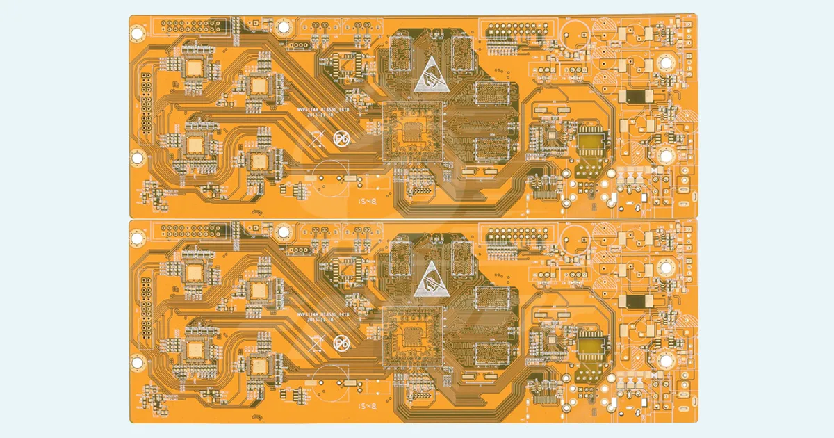
SprintPCB: Leading Rigid Flex PCB Manufacturer
SprintPCB is a premier Rigid Flex PCB manufacturer located in China, with over 17 years of experience in Rigid Flex PCB manufacturing. We pride ourselves on our ability to communicate effectively with customers, ensuring that we meet their needs from the early design stages through to final production.
Our factory is both UL and ISO9001:2015 certified, guaranteeing the highest quality standards. Our extensive experience and efficient Rigid Flex PCB manufacturing process allow us to offer competitive pricing without compromising on quality. We are dedicated to providing high-quality Rigid Flex PCBs that meet the diverse needs of our global clientele.
In conclusion, SprintPCB’s comprehensive Rigid Flex PCB manufacturing process ensures the production of reliable and high-performance PCBs. Our commitment to quality, combined with competitive pricing, makes us a trusted partner for businesses seeking superior Rigid Flex PCBs.