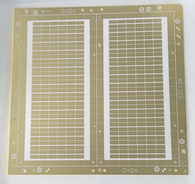
In PCBs, microvias not only improve space utilization but also serve as one of key processes for enhancing PCB density and performance. They have become an essential option for high-frequency, high-density circuit board manufacturing. This article will delve into stacked microvia (Stacked Via) and offset microvia (Offset Via) technologies in PCBs. Drawing on Shenzhen SprintPCB's practical experience, this article will help you better understand the application and advantages of these technologies in high-precision, high-performance circuit boards.


Stacked Via refers to the process of achieving electrical connection between different layers in PCB design by stacking multiple hole layers at the same location.
Space Saving: The stacked microvia design allows multiple electrical connections to be concentrated in a single area, reducing the number of vias on the board and saving space. This is particularly important for high-density and miniaturized circuit boards, effectively increasing PCB routing density and meeting the demanding space requirements of modern electronic products.
Increasing Multilayer Board Production Density: Stacked microvias concentrate multiple through-holes in a single location, allowing more signal traces to be arranged within the same area, thereby increasing the production density of multilayer PCBs. For complex circuit boards requiring a large number of connection points, the stacked microvia design provides an effective solution.
Supporting High-Speed Signal Transmission: The stacked microvia design reduces signal path length, thereby increasing signal transmission speed. This is particularly important for high-frequency circuit boards, effectively reducing delays and distortion in signal transmission, ensuring board reliability and performance.
Optimizing Electrical Performance: The stacked microvia design makes electrical connections across multiple layers more compact, reducing crosstalk and mutual interference between signal traces, thereby optimizing electrical performance. For high-frequency and high-speed applications, stacked microvias provide better impedance control and reduce signal loss.
Improved manufacturing flexibility: Stacked microvias can be flexibly designed between different layers, and different electrical connections can be achieved through different stacking combinations, which provides designers with more flexibility and helps better meet the needs of different customers.

Offset Via, also known as staggered microvia or stepped microvia, refers to a multi-layer PCB in which the microvias between adjacent layers are not completely stacked vertically on the same axis, but are staggered in a stepped manner, forming a "stepped" or "step stacked" structure.
Reduced Processing Risk: Compared to stacked microvias, which require multiple, highly precise stacking alignments and plating, staggered microvias utilize a stepped, layer-by-layer connection, avoiding the risks of hole offset and poor plating associated with higher-level stacking. This allows for a more controllable production process.
Improved Yield: During manufacturing, staggered microvias feature shorter individual via segments, making plating and filling each segment less challenging and resulting in a higher overall yield. This is particularly important for mass production, effectively controlling costs and ensuring batch consistency.
Relatively Low Cost: Compared to high-level stacked microvias, staggered microvias offer a more mature processing technology and less stringent equipment precision requirements, reducing single-board manufacturing costs. They are suitable for cost-sensitive products that still require high-density wiring.
Strong Applicability: The staggered microvia design offers flexibility and allows for optimal placement of stepped locations based on circuit requirements and layout, making it suitable for a variety of HDI designs. It is particularly widely used in thin and lightweight products such as smartphones, wearables, and automotive electronics.
Stacked microvias pursue direct vertical connections. Multiple microvias are stacked and aligned to create a more compact routing channel within a vertical space. This approach is suitable for high-end designs requiring extremely compact space and shortest signal paths.
Offset microvias achieve deep connections through a stepped offset pattern, staggering the connection points at different levels. This is more suitable for balancing routing density and manufacturability, reducing the manufacturing complexity associated with stacking.
Stacked vias require high-precision alignment and multiple electroplating and filling stages. Inadequate inter-layer alignment or filling can result in internal via short circuits or poor solder joints between layers. Therefore, the manufacturing process and inspection requirements are extremely high.
Each connection stage of an offset via is relatively simple. After partial press-fitting, the next hole is drilled to connect. The next hole is located at an offset position. This allows for greater inter-layer alignment tolerance, improved process stability, and a higher yield rate.
Stacked vias require multiple drilling, plating, filling, and alignment steps, resulting in a long processing cycle and relatively higher manufacturing costs. The offset micro-hole process is relatively mature, with slightly lower reliance on laser drilling equipment and more manageable overall costs, making it suitable for mass production and cost-sensitive projects.
| Category | Stacked Via | Offset Via |
| Typical Applications | High-end smartphones, chip carriers, high-speed communication devices | Mid-to-high-end smart terminals, consumer electronics, automotive electronics |
| Layer Count | High-density multilayer, 6 layers and above HDI boards | Mainstream 4–8 layer HDI boards |
| Signal Requirements | High frequency, high speed, low latency | Medium-to-high speed, emphasis on cost-effectiveness and efficiency |
| Design Priorities | Minimizing space, performance priority | Cost control, manufacturability priority |
In terms of production capacity, Shenzhen SprintPCB has introduced multiple high-precision drilling machines, LDI exposure equipment and automated lamination production lines to ensure high consistency and reliability in micro-via drilling, hole filling, electroplating and lamination processes. Facing high-frequency, high-density, and high-quality PCB orders, Shenzhen SprintPCB can stably achieve:
Microvia diameters as small as 0.15mm, with layer-to-layer alignment precision within 1 mil;
Mass production of hybrid stacked + offset via structures for 6-layer, 8-layer, 12-layer+ designs;
Strict impedance control and low-loss dielectric stack-ups for high-speed signal transmission;
Flexible delivery for both prototypes and small to mid-volume production, including expedited turnaround.
Whether you require complex multilayer boards or high-speed designs with stringent signal integrity, choosing SprintPCB means choosing precision manufacturing, dependable quality, and competitive delivery efficiency.

Customer support