In PCB design, power planes are a critical component. Their main function is to provide reliable power and ground connections to ensure the performance and reliability of the circuit board. Here are some best practices for power plane PCB design:
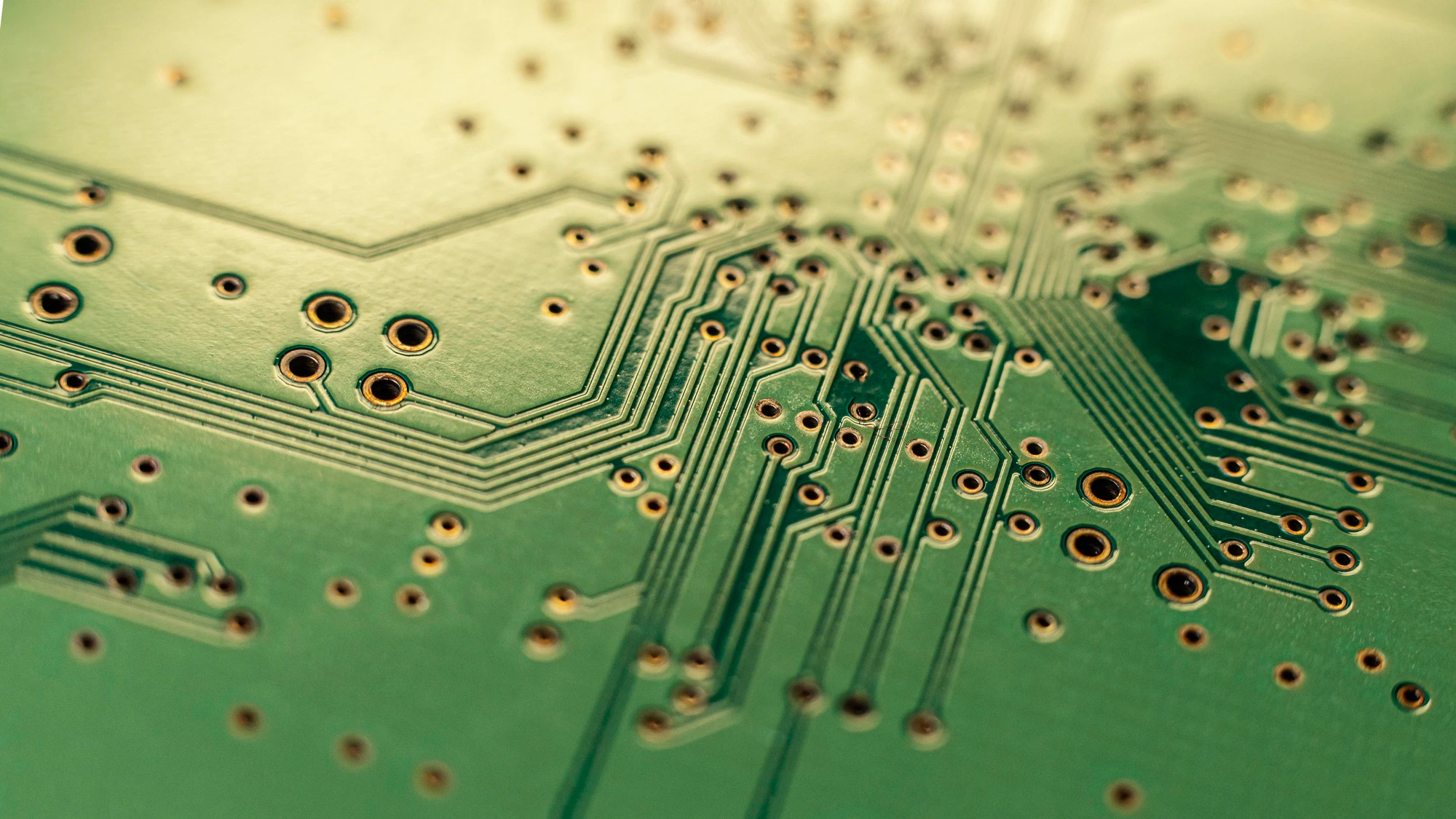
- Use a layered plane design in the PCB. In complex PCBs, creating separate planes for power and ground can help reduce noise and interference, as well as provide a low impedance path for current.
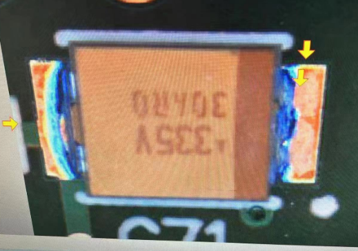
- Ensure proper placement and sizing of power and ground vias. Vias should be placed near components that require a strong connection to the power or ground plane. They should also be sized appropriately for the current being carried.
- Avoid creating isolated islands of copper in the power plane. These can create hot spots and increase the risk of failure. Instead, design the power plane to have a continuous flow of copper.
- Use multiple vias for high current connections. For components that require high current, such as voltage regulators and power connectors, multiple vias should be used to ensure sufficient current carrying capacity.
- Consider thermal management in the power plane design. Power dissipation can cause temperature rise in the PCB, which can affect the performance and reliability of the circuit. Thermal vias and heatsinks can be used to manage heat in the power plane.
By following these best practices, designers can ensure the reliability and performance of their power plane PCB designs.