Reverse engineering a PCB can help us understand the design of an existing PCB, which is extremely useful for designing new products, modifying old products, or cracking competitors' products. However, reverse engineering a PCB is not an easy task and requires patience and professional knowledge. In this article, we will discuss the basic steps of reverse engineering a PCB.
Step 1: Collect Information
Before reverse engineering a PCB, we need to collect as much information as possible. This includes the PCB specification sheet, schematic diagram, bill of materials, and markings on the PCB, among others. This information can help us better understand the design of the PCB.
Step 2: Analyze the PCB
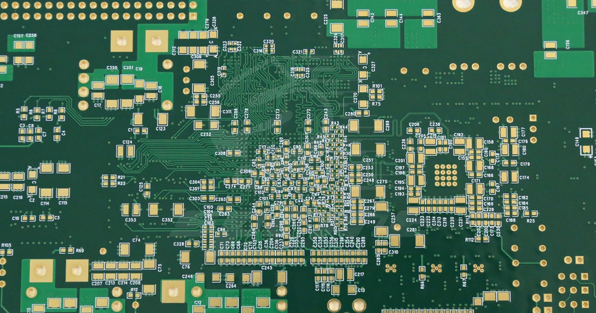
Once we have collected enough information, we need to start analyzing the PCB. This includes examining all the components on the PCB, understanding their functions and connections. We also need to inspect all the traces and circuits on the PCB to determine their connections and signal transmission paths.
Step 3: Draw a Schematic Diagram
After analyzing the PCB, we need to draw a schematic diagram. This can help us better understand the circuit and determine the function and connection of each component. For complex PCBs, this may take some time and effort.
Step 4: Rebuild the PCB
After drawing the schematic diagram, we need to rebuild the PCB. This can help us better understand the PCB design and determine the layout and connections of the PCB. For complex PCBs, this may require some specialized tools and skills.
Step 5: Test the PCB
Finally, we need to test the PCB. This can help us determine whether the functionality of the PCB matches the original design and identify any potential problems. Before testing the PCB, we need to ensure that all the components on the PCB are properly connected and that the layout and connections of the PCB match the original design.
Conclusion: Reverse engineering a PCB can help us understand the design of an existing PCB, but it is not an easy task and requires patience and professional knowledge. By following the five steps of collecting information, analyzing the PCB, drawing a schematic diagram, rebuilding the PCB, and testing the PCB, we can better complete the task of reverse engineering a PCB.