Recently we have been doing ESD tests for electronic products. From the test results of different products, we found that this ESD is a very important test: if the circuit board design is not good, the introduction of static electricity will cause product crashes or even component damage. Before, I only noticed that ESD would damage components, but I didn't expect that we should also pay enough attention to electronic products.
ESD, also known as electrostatic discharge. According to the knowledge learned, static electricity is a natural phenomenon, usually generated by contact, friction, induction and other methods between electrical appliances. Its characteristics are long-term accumulation, high voltage (can produce thousands of volts or even tens of thousands of volts of static electricity), small amount of electricity, small current and short action time. For electronic products, if ESD design is not done well, electronic and electrical products tend to be unstable or even damaged. There are usually two methods for ESD discharge test: contact discharge and air discharge. Contact discharge is direct discharge to the device under test; air discharge also known as indirect discharge is caused by strong magnetic field coupling to adjacent current loop. The test voltage of these two tests is generally 2KV-8KV and different regions have different requirements. Therefore before designing it is necessary to understand the PCB market targeted by the product. The above two situations are basic tests for electronic products when human body contacts electronic products and cannot work due to human body electrification or other reasons.
The humidity situation in different parts of the world is different but at the same time if the air humidity in a region is different the static electricity generated will also be different. The following table shows the data collected from which we can see that static electricity increases with decreasing air humidity. This also indirectly explains why there are large sparks from static electricity when removing hair in winter in northern China. Since static electricity has such great harm how should we protect it? We usually take three steps when designing electrostatic protection: prevent external charge from flowing into circuit board causing damage; prevent external magnetic field from damaging circuit board; prevent danger caused by electrostatic field.
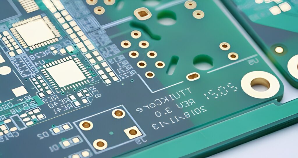
In actual PCB circuit design we will use one or more of the following methods for electrostatic protection:
1、Avalanche diode for electrostatic protection: This is also a common method used in design. The typical method is to parallel an avalanche diode to ground on key signal lines. This method uses avalanche diode's fast response and stable clamping ability which can consume accumulated high voltage in a short time to protect circuit board.
2、Circuit protection using high voltage capacitor: In this approach ceramic capacitors with withstand voltage of at least 1.5KV are usually placed at I/O connectors or key signal positions and wires are kept as short as possible to reduce wire inductance. If capacitors with low withstand voltage are used they will damage capacitors and lose protection effect.
3、Use ferrite beads for circuit protection: Ferrite beads can attenuate ESD current and suppress radiation. When faced with two problems ferrite beads are a good choice.
4、Spark gap method: This method can be seen in one piece material. The specific method is that microstrip layer composed of copper sheet consists of triangular copper sheet whose tips align with each other. One end of triangular copper sheet connects signal line and other end connects ground. When there is static electricity there will be tip discharge consuming electric energy.
5、Use LC filter to protect circuit: LC filter can effectively reduce high frequency static electricity entering circuit. Inductance reactance can well prevent high frequency ESD from entering circuit while capacitor shunts high frequency energy of ESD to ground.At same time this kind of filter can smooth signal edge reduce radio frequency influence improve performance in signal integrity aspect further.
6、Multi-layer PCB board ESD protection: Choosing multi-layer board is also an effective way to prevent ESD when funds permit.In multi-layer boards because there are complete ground planes near wiring ESD can couple faster to low impedance plane thus protecting key signals.
7、Retention method for protective tape around PCB line board: This method is usually used to draw wiring without assembly and soldering layer around circuit board.If conditions permit connect wiring to shell.At same time pay attention not to form closed loop so as not to form ring antenna causing more trouble
8、Circuit protection using CMOS devices or TTL devices with clamping diodes: This method uses isolation principle to protect circuit board.Because these devices have clamping diodes protection it reduces complexity of design in actual circuit design
9、Frequently use decoupling capacitors: These decoupling capacitors should have low ESL and ESR values.For low frequency ESD decoupling capacitors reduce loop area.

Customer support