Differences and Advantages of HDI PCBs Compared to Regular PCBs:
Size and Weight
HDI PCB: Smaller and lighter. Due to the use of high-density wiring and finer line widths and spacings, HDI PCBs can achieve a more compact design. This makes them particularly suitable for modern electronic devices that require miniaturization and lightness.
Regular PCB: Typically larger and heavier, suitable for simpler and lower-density wiring needs. They are commonly used in applications where space and weight are not as critical.
Materials and Structure
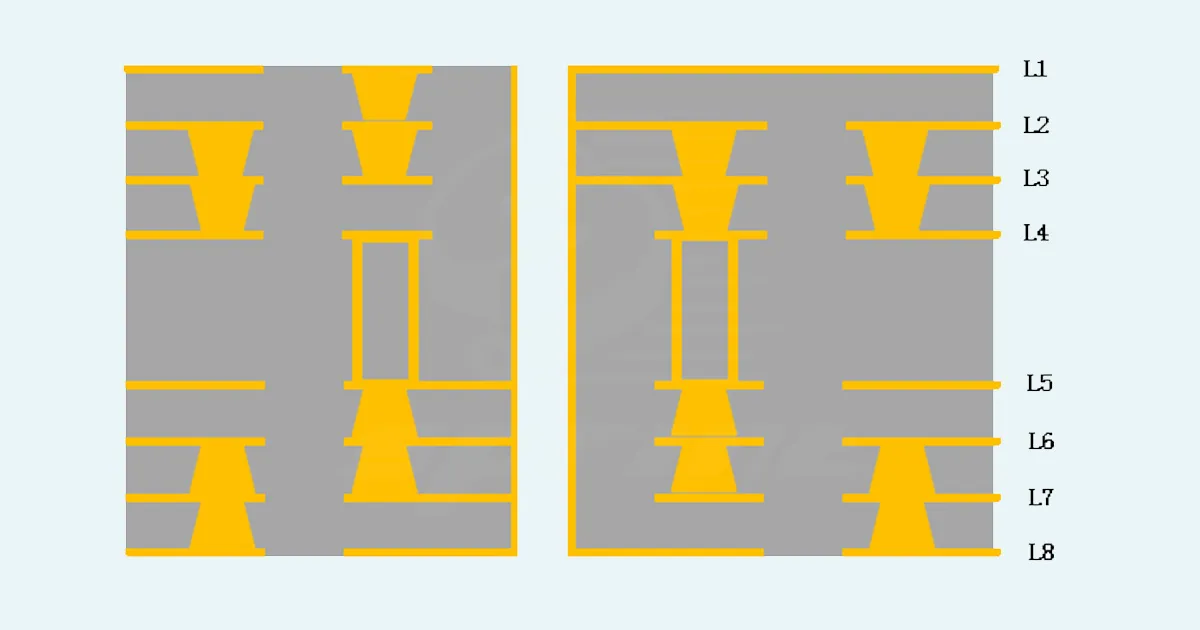
HDI PCB: Usually utilizes a double-sided board as the core, then builds up multiple layers through sequential lamination, known as "Build-Up Multilayer" (BUM) technology. Electrical connections between layers are achieved using numerous tiny blind and buried vias. This advanced structure enables the complex interconnections required by high-performance devices.
Regular PCB: Traditional multilayer structure mainly connects layers through through-holes, and can also use blind and buried vias, but the design and manufacturing process are relatively simple. The via sizes are larger and the wiring density is lower, making them suitable for low to medium-density applications.
Manufacturing Process
HDI PCB: Employs laser drilling technology to create smaller blind and buried vias with diameters less than 150um. This process requires high precision in hole positioning, as well as stringent control over costs and production efficiency. The advanced equipment and techniques involved highlight the expertise of
China HDI PCB manufacturers in delivering cutting-edge solutions.
Regular PCB: Primarily uses mechanical drilling technology, with typically larger via diameters and layer counts. This traditional method is less complex and suitable for less demanding applications.
Wiring Density
HDI PCB: Higher wiring density, with line widths and spacings usually not exceeding 76.2um, and a solder pad density greater than 50 per square centimeter. This high density allows for more connections and components in a smaller area, enhancing the functionality and performance of electronic devices.
Regular PCB: Lower wiring density, with wider line widths and spacings, and a lower solder pad density. This is adequate for applications with less stringent performance requirements.
Dielectric Layer Thickness
HDI PCB: Thinner dielectric layers, typically less than 80um, with higher demands for uniform thickness, especially in high-density boards and substrates requiring impedance control. This contributes to better signal integrity and performance in complex electronic circuits.
Regular PCB: Thicker dielectric layers, with relatively lower requirements for uniformity. This is sufficient for applications where signal integrity is not as critical.
Electrical Performance
HDI PCB: Superior electrical performance, capable of enhancing signal strength and reliability. HDI PCBs offer significant improvements in terms of radio frequency interference (RFI), electromagnetic interference (EMI), electrostatic discharge (ESD), and thermal conductivity. These attributes make them ideal for high-performance and sensitive electronic applications.
Regular PCB: Lower electrical performance, suitable for applications with less demanding signal transmission requirements.
Design Flexibility
HDI PCB: Due to its high-density wiring design, HDI PCBs enable more complex circuit designs within limited space. This provides designers with greater flexibility to add more features and functionality without increasing the size of the PCB. The advanced design capabilities of China HDI PCB manufacturers allow for innovative solutions that meet the evolving needs of the electronics industry.
While HDI PCBs offer clear advantages in terms of wiring density, electrical performance, and size, their manufacturing process is more complex and requires higher technical capabilities. Techniques such as laser drilling, precise alignment, and microvia filling necessitate advanced technical support, which also leads to higher production costs. In contrast, traditional multilayer PCBs, with their simpler structure and lower manufacturing demands, are suitable for low to medium-density applications.
HDI PCBs from China HDI PCB manufacturers provide higher wiring density, superior electrical performance, and smaller size, making them ideal for high-end applications. However, their complex manufacturing processes and higher costs must be considered. Traditional multilayer PCBs, while less advanced, remain a viable option for less demanding applications.