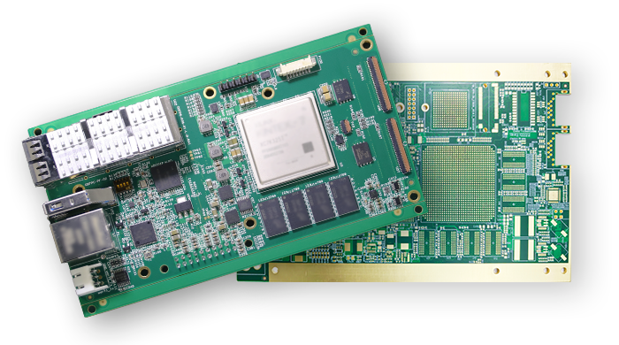
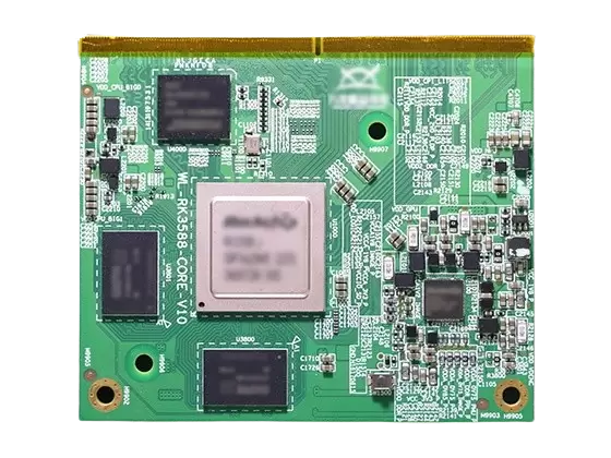
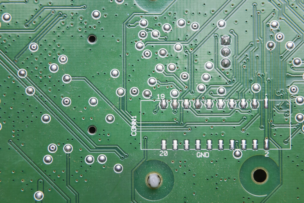
Have you ever wondered what those green coatings and white markings in electronic devices are for? When you disassemble an electronic device or carefully examine your electronic prototype board, you may notice a layer of green coating on the solder pads and white markings on the circuit board.
These green coatings are called solder masks, and the white markings are PCB silkscreens. Although they are relatively small in electronic device manufacturing, they play a very important role. This article will introduce the functions of solder masks and PCB silkscreens, as well as the benefits they bring to the electronic manufacturing process.
Before delving into the importance of solder mask and PCB silkscreen, let's first understand their respective definitions and functions. This will help us gain a better understanding of their roles in electronic manufacturing.
What is a solder mask?
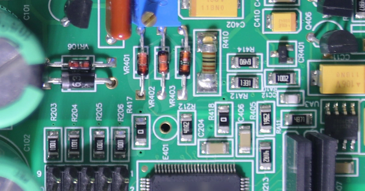
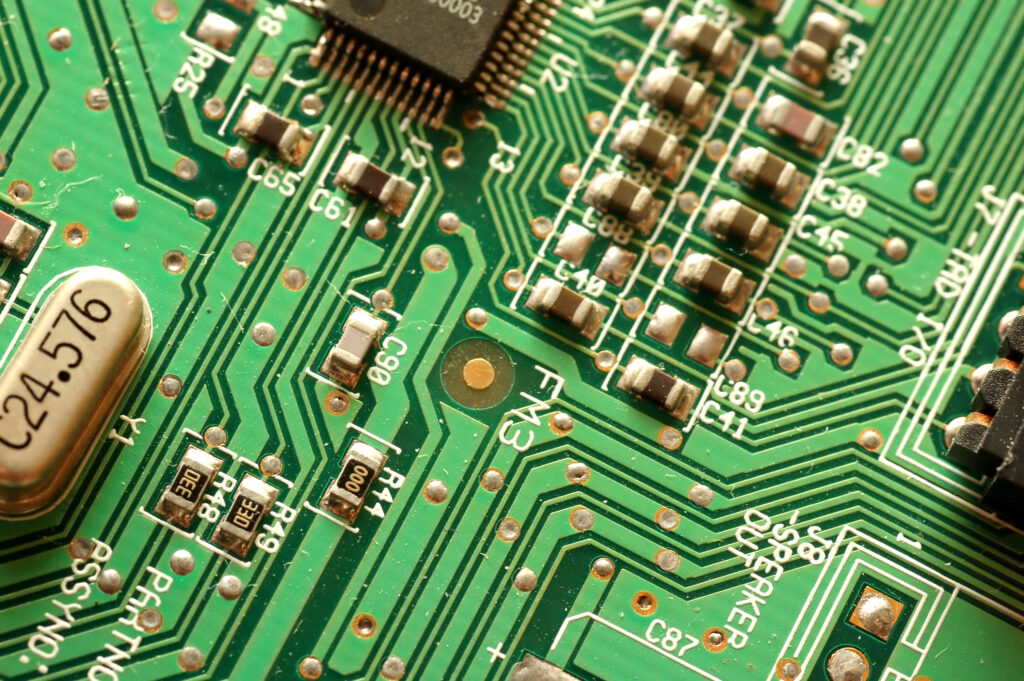
A solder mask is a coating applied to a printed circuit board (PCB), typically in green color. It is applied to the solder pad areas, which are the metal pad areas between component pins and the PCB. Solder masks are usually made of polyimide or epoxy resin and are applied as a layer over the copper foil on the PCB.
The main function of solder mask is to protect the solder pads from external environmental corrosion and damage. It forms an insulating layer that can prevent short circuits, electrical interference, as well as damage caused by oxidation or corrosion during the soldering process. The coating of the solder mask can also reduce solder bridging and errors during the soldering process, ensuring the accuracy and reliability of the solder joints.
The solder mask plays a vital role in the PCB manufacturing and assembly processes.
As a protective layer, the solder mask prevents the solder pads from encountering corrosive substances, dust, moisture, and contaminants that may be present in the external environment.
This helps maintain the reliability and durability of the solder pads and extends the lifespan of the circuit board.
The insulating properties of solder mask effectively prevent short circuits between different solder pads, avoiding the formation of incorrect current paths. It also reduces the likelihood of electromagnetic interference (EMI) and radio frequency interference (RFI), thereby enhancing the circuit board's immunity to interference.
The coating on the solder mask controls the flow of solder, reducing soldering errors and the risk of short circuits between solder pads. It provides precise guidance to limit the solder's position, making the soldering process more controlled and accurate.
Solder mask is widely used in various electronic devices and industries, including but not limited to:
Communication equipment: Solder mask is used in the PCB manufacturing and assembly processes of mobile phones, routers, communication base stations, and other devices, ensuring their stability and reliability in various environments.
Automotive Electronics: In the field of automotive electronics, solder mask is used to manufacture and assemble vehicle control units, instrument clusters, in-car entertainment systems, and more, to ensure their normal operation under harsh vibration, temperature, and humidity conditions.
Industrial Control Systems: Solder mask is applied to PCBs in industrial automation and control systems to protect circuit boards from dust, moisture, and chemical substances present in industrial environments, ensuring the reliability and stability of the equipment.
Medical Equipment: In the manufacturing of medical devices, the solder mask is used on PCBs for various medical equipment to prevent the impact of bacteria, corrosive liquids, and environmental contamination on device performance and patient safety.
In summary, the solder mask plays a crucial role in electronic device manufacturing across various fields. It protects the solder pads, enhances the stability and reliability of circuit boards, while reducing soldering defects and maintenance costs. It is an indispensable component in modern electronic manufacturing.
Now that we have understood the role of the solder mask, let's turn our attention to PCB silkscreens and understand their importance.
What are PCB silkscreens?
PCB silkscreen refers to the white markings printed on a circuit board, typically created using the silk-screen printing technique. They are visible marks used for identification and guidance to aid in assembly, testing, and repair processes during electronic manufacturing. Silkscreen typically includes text, symbols, pin labels, component placements, and other relevant information, which can be directly printed on the surface of the circuit board or on top of components.
The silk screen printing on PCB plays an important role in electronic manufacturing.
PCB silk screen printing provides textual and symbolic markings to aid in identifying and locating components, connectors, test points, and other critical features on the circuit board. This is particularly important for assembly personnel as they can correctly install and connect components based on the silk screen instructions, thereby reducing the risk of assembly errors.
Additionally, silk screen printing provides useful references for repair and troubleshooting, making it easier to locate and fix issues.
The silk screen printing on PCBs can enhance the visual texture of circuit boards and give electronic products a professional and high-quality appearance. The precise markings and clearly visible information provided by silk screen printing can increase the visual appeal of the product and enhance the user experience.
Additionally, silk screen printing can be used to incorporate brand logos and meet customization requirements using different colors and fonts, giving the product unique visual characteristics.
PCB silkscreen provides a visual representation of crucial information, making it easier to read and comprehend circuit boards. By marking component pins, connection points, voltage, and signal names, among other important details, silkscreen aids engineers and technicians in quickly understanding the functionality and design intent of the circuit board. This is essential for the development, testing, and maintenance of electronic systems, as it helps reduce errors and improve efficiency.
PCB silk screen printing is widely used in various electronic devices and systems, including but not limited to the following fields:
Consumer Electronics: PCB silk screen printing is commonly found in consumer electronic products such as mobile phones, tablets, televisions, audio devices, and household appliances. They help users identify and operate various functional buttons, connectors, and indicator lights.
Industrial Control: In industrial automation and control systems, PCB silkscreen is used to identify key components such as sensors, actuators, controllers, and connectors, to assist engineers in proper wiring and debugging.
Medical Equipment: In the medical industry, PCB silk-screen printing is crucial for identifying different functional areas, control panels, and warning signs on medical devices. They provide essential guidelines for healthcare workers to operate the equipment correctly and adhere to specific safety guidelines.
Automotive Electronics: In the field of automotive electronics, PCB silk screening is used to identify key components such as control units, sensors, wiring harnesses, and connectors in automotive electronic systems. They assist technicians in diagnostics, repairs, and maintenance work.
In summary, PCB silk screen plays a crucial role in electronic manufacturing by providing identification, guidance, and legibility, thereby enhancing the functionality and visual effects of circuit boards. Whether in consumer electronics, industrial control, medical devices, or automotive electronics, PCB silk screen plays a key role in ensuring the performance and reliability of electronic products.
Through our introduction to the solder mask and the PCB silk screen, we can see their importance in electronic manufacturing. Now, let's summarize their benefits.
Solder mask and PCB silkscreen play a crucial role in protecting circuit boards and solder pads. A solder mask is a layer of coating applied to the solder pads, which prevents excessive solder paste from flowing around the pads during soldering, thereby avoiding short circuits and soldering defects.
It also acts as a barrier against air, humidity, and other environmental factors that can cause corrosion and oxidation of the circuit board, thus extending its lifespan. The solder mask also provides insulation properties, preventing electrical short circuits between solder pads.
In addition, it can also provide a certain degree of mechanical protection, reducing the impact of external physical damage on the circuit board. In summary, the solder mask ensures the normal operation of the circuit board and solder pads in various environments by providing a protective layer, thereby improving the reliability and stability of the equipment.
Solder mask and PCB silkscreen play a crucial role in the electronic manufacturing process, significantly improving manufacturing efficiency. The presence of solder mask makes the soldering process easier and more precise. It can restrict the flow of solder paste, making component placement on the solder pads simpler. The existence of a solder mask also reduces solder paste wastage during the soldering process, enhancing production efficiency and lowering costs.
Additionally, PCB silkscreen serves as a labeling and guiding tool, aiding manufacturing personnel in accurate positioning and installation of electronic components, reducing the possibility of assembly errors. By providing clear instructions and markings, PCB silkscreen makes the manufacturing process more efficient, accurate, and controllable.
Silkscreen printing on PCBs plays an important role in electronic manufacturing by providing identification and guidance. Silkscreen markings typically appear on the circuit board in the form of white symbols, text, or graphics.
They can be used to identify important locations such as components, connectors, and test points on the PCB. These markings assist manufacturing personnel in accurately identifying and locating components during assembly and testing, thereby reducing errors and improving efficiency.
Additionally, PCB silkscreen printing can include version numbers, manufacturer information, and other important identifiers, facilitating post-sales maintenance and troubleshooting. Through clear identification and guidance, PCB silkscreen printing helps ensure the quality and consistency of circuit boards, simplifies the manufacturing process, and enhances product traceability.
As discussed in this article, the solder mask and PCB silkscreen play a crucial role in electronic manufacturing. The solder mask protects the circuit board and solder pads, preventing short circuits and environmental corrosion.
Meanwhile, the PCB silkscreen provides identification and guidance, making the electronic manufacturing process more efficient and precise. These small green coatings and white markings play a key role in the performance and reliability of electronic devices. Therefore, whether in personal DIY projects or large-scale production, the solder mask and PCB silkscreen are indispensable.
Transform Your PCB Manufacturing with SprintPCBSprintPCB is a renowned high-tech enterprise specializing in delivering exceptional PCB manufacturing services to global clients. With our extensive industry knowledge and competitive pricing, you can shift your attention towards the most vital elements of your organization. Get in touch with us today to explore the potential for collaboration and experience how we can help you surpass your goals.