Electroless Nickel Immersion Gold (ENIG) is one of the most widely adopted surface finishing processes in
PCB manufacturing. It is valued for its ability to provide a flat, durable, and solderable surface, making it indispensable for advanced applications like
multilayer PCBs, high-frequency circuits, and high-reliability electronics. In this article, we explore the ENIG process in detail, including its principles, benefits, and the steps involved in achieving this precise finish.
What Is the ENIG Process?
ENIG is a dual-layer surface treatment that combines a nickel barrier and a thin layer of gold over the copper traces of a PCB. The nickel acts as a barrier to prevent copper diffusion and serves as a solid base for soldering, while the gold protects the nickel from oxidation and ensures a long-lasting, solderable surface.
Unlike electroplating, ENIG is an electroless process, which means the deposition occurs through chemical reactions rather than electric current. This ensures uniform coverage even on complex PCB designs.
Benefits of the ENIG Process
Flat and Uniform Surface
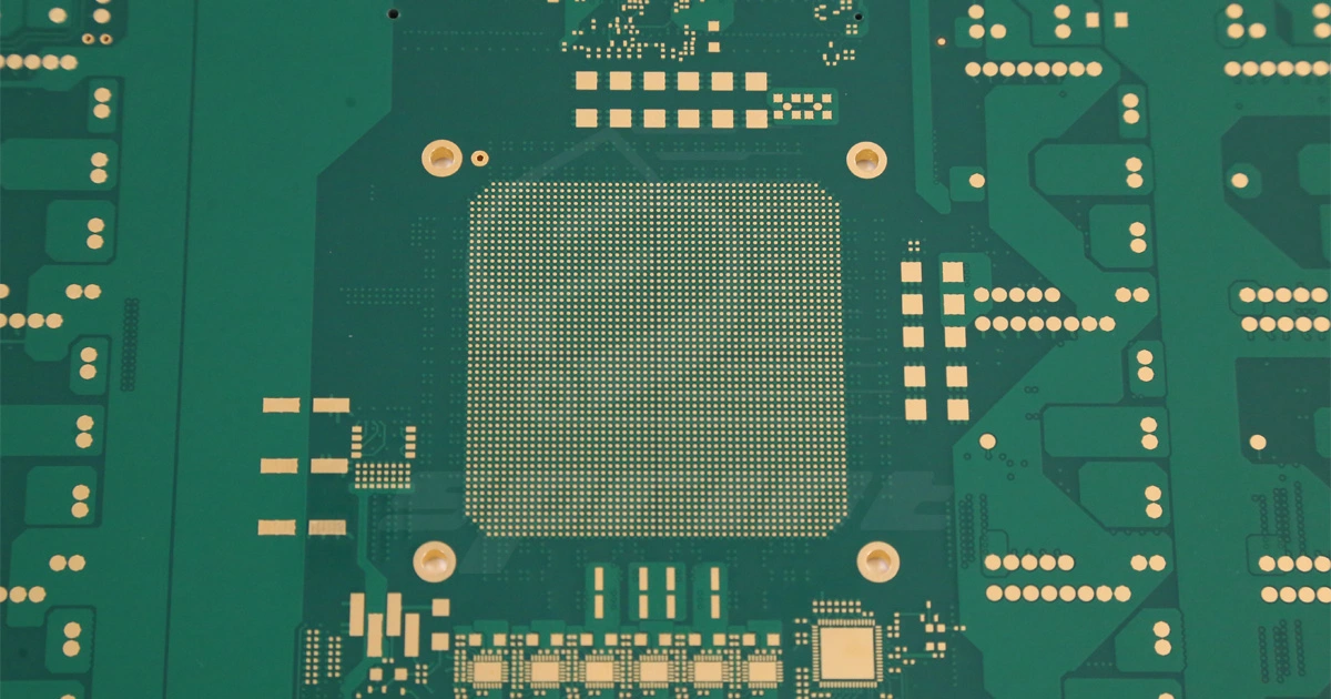
ENIG creates a flat, smooth surface, essential for surface-mount technology (SMT) and high-density interconnects (HDI). This flatness is critical for advanced packaging like Ball Grid Arrays (BGA) and fine-pitch components.
Superior Solderability
The gold layer ensures excellent solder joint quality, reducing the risk of brittle connections. This makes ENIG ideal for applications where reliability is paramount.
Corrosion Resistance
The nickel layer provides strong protection against environmental conditions like moisture and oxidation, extending the PCB’s lifespan.
Compatibility with Lead-Free Processes
ENIG is RoHS-compliant and environmentally friendly, making it suitable for modern manufacturing practices.
Long Shelf Life
ENIG-coated PCBs can be stored for extended periods without degrading solderability, a key advantage in industries with long production cycles, such as aerospace and medical devices.
Detailed ENIG Process Steps
The ENIG process involves a series of chemical treatments to ensure precise and consistent results. Below is a step-by-step breakdown:
Surface Cleaning
The copper surface is thoroughly cleaned to remove contaminants, oxidation, and residues. This step typically involves:
Chemical Degreasing: Removes oils and organic residues.
Micro-etching: Creates a fresh, clean copper surface for optimal adhesion.
Pre-activation
The cleaned copper is treated with a pre-activator solution to enhance the deposition process. This step prepares the surface for uniform nickel deposition.
Catalyst Application
A palladium-based catalyst is applied to the copper surface. Palladium acts as a seed layer that initiates the electroless nickel plating process.
Electroless Nickel Plating
The copper is submerged in a nickel bath containing nickel salts and reducing agents (e.g., sodium hypophosphite). A chemical reaction deposits a uniform nickel layer, typically 3–6 microns thick, onto the copper. The nickel layer acts as a barrier to prevent copper migration and provides a strong, solderable surface.
Immersion Gold Plating
The board is then dipped into an immersion gold bath. This process uses a displacement reaction where gold ions replace nickel atoms on the surface, forming a thin gold layer of about 0.05–0.1 microns. The gold protects the nickel from oxidation and ensures excellent bonding properties.
Rinsing and Drying
After plating, the PCB is thoroughly rinsed to remove residual chemicals. It is then dried to prepare for the next stages of production or storage.
Applications of ENIG Process
Multilayer PCBs
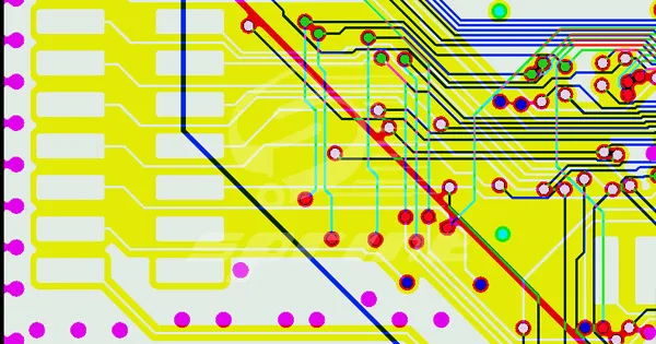
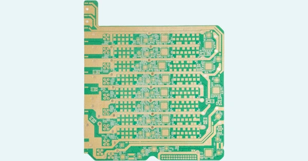
The ENIG finish is especially beneficial for multilayer PCBs, where precise layer alignment and flat surfaces are crucial. Its uniformity ensures error-free assembly, even with complex HDI designs.
High-Frequency Circuits
ENIG’s smooth surface minimizes signal loss and impedance variations, making it ideal for RF and microwave applications.
Mission-Critical Applications
Industries such as aerospace, automotive, and medical electronics rely on ENIG for its durability and reliability under extreme conditions.
Addressing Limitations
While ENIG offers numerous advantages, it has potential drawbacks:
Black Pad Defect: Caused by excessive phosphorus in the nickel layer, leading to weak solder joints. This issue can be mitigated through strict process control and monitoring.
Higher Cost: Compared to simpler finishes like HASL (Hot Air Solder Leveling), ENIG is more expensive. However, its superior performance and compatibility with advanced designs justify the investment.
Why Choose SprintPCB for ENIG Solutions?
As a leading PCB manufacturer, SprintPCB specializes in delivering high-quality PCBs with ENIG finishes. Our state-of-the-art facilities and stringent quality control ensure precision and reliability in every product. Whether for consumer electronics or high-reliability industrial applications, SprintPCB provides customized solutions to meet your needs.