SprintPCB's HDI Multilayer PCB technology, with its unique advantages in miniaturization, high performance, and energy efficiency.Introduction
In the electronics industry,
HDI Multilayer PCB technology is used more and more widely. This technology provides the possibility for miniaturization and high performance of electronic equipment with its high-density interconnection performance and excellent electrical performance. As a high-tech enterprise committed to providing customers with one-stop high-end printed circuit board manufacturing services from R&D samples to mass production, SprintPCB Company 1 has rich experience and deep technical accumulation in the application of HDI Multilayer PCB technology.
Introduction to HDI Multilayer PCB technology
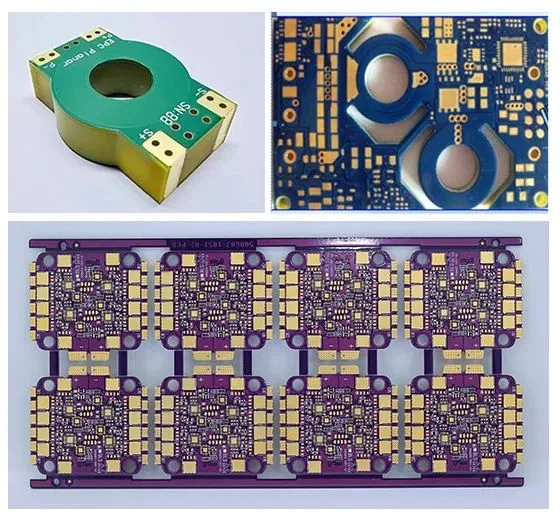
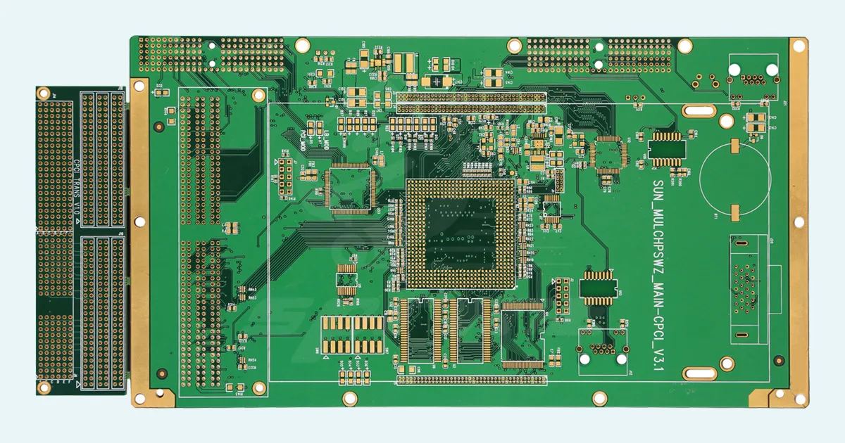
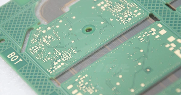
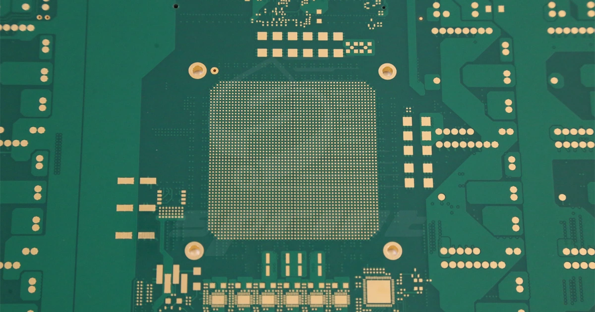
HDI Multilayer PCB is a printed circuit board manufactured using micro-hole and thin material technology. It is characterized by very small line width, line spacing and aperture, so it can achieve more functions in a limited space.
Structure of HDI Multilayer PCB
HDI Multilayer PCB is usually composed of multiple layers of insulating materials and conductive layers stacked alternately, and each layer is connected to each other through micropores. This structure enables HDI Multilayer PCB to have excellent signal transmission performance and extremely high integration.
Advantages of HDI Multilayer PCB technology
Miniaturization and lightweight
Due to the high-density characteristics of HDI Multilayer PCB, more functions can be implemented in a smaller space, thus greatly reducing the size and weight of electronic equipment.
High performance
HDI Multilayer Pcb's micropore and thin material technology enables faster and more stable signal transmission, thereby improving the performance of electronic devices.
Energy saving and environmental protection
The high efficiency and low power consumption characteristics of HDI Multilayer PCB can not only save energy, but also be beneficial to environmental protection.
Conclusion
SprintPCB's HDI Multilayer PCB technology is gradually changing the face of the electronics industry with its unique advantages. With the advancement of technology, SprintPCB Company's HDI Multilayer PCB technology will play a greater role in the future. SprintPCB is committed to providing rapid electronic manufacturing services to more than 3,000 customers around the world, and looks forward to cooperating with more customers to jointly promote the development of the electronics industry.