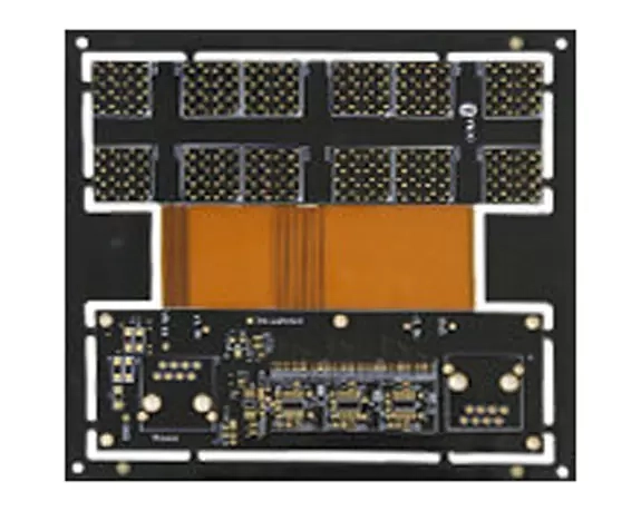
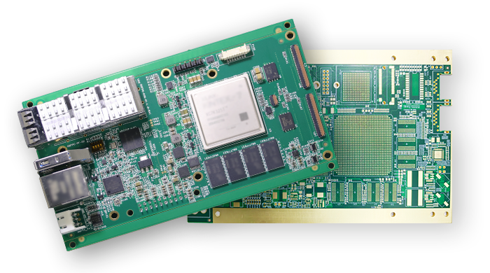
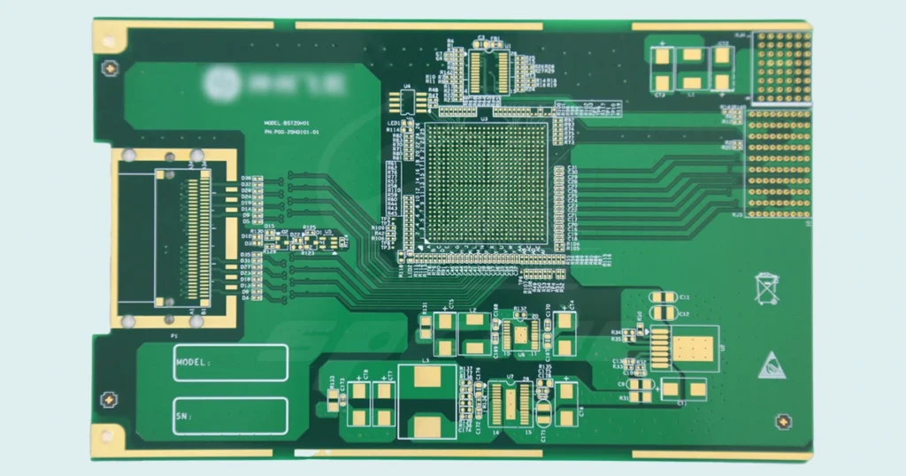
SprintPCB provides high-quality Multilayer PCB Board manufacturing services, from design to testing, ensuring optimal performance and reliability. In modern electronic equipment, Multilayer PCB Board is used more and more widely. As a professional PCB manufacturer, SprintPCB has more than 17 years of professional service experience, providing high-quality PCBs of various types and complexity to thousands of satisfied companies around the world. This article will combine SprintPCB's professional knowledge and experience to introduce the manufacturing process of Multilayer PCB Board in detail.
Design stage
Electronic engineers need to use specialized computer-aided design (CAD) software to design the circuit diagram of the Multilayer PCB Board. At this stage, factors such as the function, performance, size, and cost of the circuit need to be considered. SprintPCB's CAD design team has rich experience and professional knowledge and can provide customers with optimal design solutions.
Plate making stage
After the design is completed, the circuit diagram needs to be converted into an actual circuit board. This process usually includes the following steps:
Image transfer
Transfer the circuit image to the copper foil-covered substrate.
Etching
Use a chemical solution to remove excess copper foil, leaving only the circuit image.
Drilling
Drill holes in the circuit board to install electronic components.
SprintPCB has an advanced PCB board manufacturing and processing factory that can complete these steps quickly and accurately.
Assembly stage
After the circuit board is completed, assembly of the electronic components can begin. This process usually includes the following steps:
SMD
attach electronic components to the circuit board.
Soldering
Use solder to secure electronic components to the circuit board.
Inspection
Use special equipment to check the performance of the circuit board to ensure there is no short circuit or open circuit.
SprintPCB's PCBA processing services cover comprehensive services such as component procurement, precision SMT, DIP, cable welding, and functional testing.
Testing Phase
The completed Multilayer PCB Board needs to be tested to ensure that its performance meets the design requirements. This process usually includes functional testing, performance testing, and durability testing. SprintPCB promises that its product safety is certified by IATF16949, ISO 9001, and UL.
The manufacturing process of Multilayer PCB board is a complex and delicate process that requires the professional knowledge and skills of electronic engineers. As a professional PCB manufacturer, SprintPCB is committed to providing customers with one-stop high-end printed circuit board manufacturing services from R&D samples to mass production. We look forward to working with you and contributing to your business success.