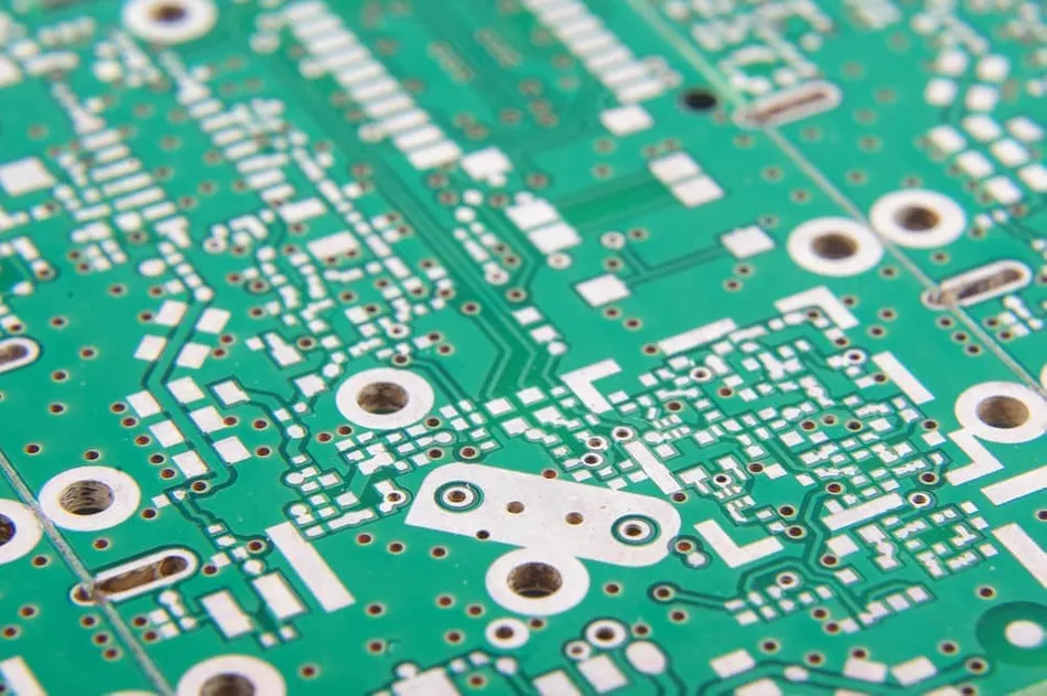
You may not often pay attention to the thickness of copper on a PCB, but in fact, it determines how much current the board can handle, how much heat it generates, and how long its service life will be.
A simple analogy:
Copper thickness = the number of lanes on a highway
Too few lanes (copper too thin): current "traffic jams," excessive heat buildup.
Too many lanes (copper too thick): current flows smoothly, but the cost rises and manufacturing becomes more difficult.
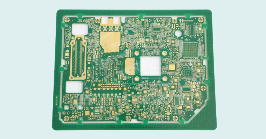
In applications such as new energy, energy storage, drones, high-power motors, and industrial power supplies, heavy copper PCBs have become almost standard. SprintPCB has mature mass production capabilities in 3oz–6oz heavy copper PCBs and has successfully delivered solutions for hundreds of high-current control and new energy projects.

In the PCB industry, copper thickness is usually expressed inounces (oz), referring to the weight of copper foil per square foot. The corresponding thickness is:
| Copper Thickness (oz) | Thickness (µm) | Common Applications |
| 0.5 oz | 17 µm | High-frequency signal boards, light-load products |
| 1 oz | 35 µm | Consumer electronics, general industrial control |
| 2 oz | 70 µm | Medium current products, power supply boards |
| 3 oz | 105 µm | High-current control boards, industrial power supplies |
| 6 oz | 210 µm | Energy storage, EV BMS, charging stations |
| 10–12 oz | 350–420 µm | Ultra-high current, special industrial equipment |
Industry note: PCBs with≥2 oz copper are generally called heavy copper PCBs, while those with>10 oz copper are classified as ultra-heavy copper PCBs.

You may consider heavy copper PCBs if your application meets one or more of the following conditions:
Current > 5A and long trace lengths
Power devices on the board generate significant heat
Product requires long-term full-load operation
Operating environment has high ambient temperatures and requires enhanced thermal dissipation
Typical applications include:
Industrial power supplies, photovoltaic inverters, and energy storage systems
EV on-board chargers (OBC), BMS, and high-voltage power distribution units
High-power motor drives, charging stations, and railway power systems
Specialized and aerospace equipment

Heavy copper not only improves current-carrying capacity but also reduces temperature rise and extends product lifespan.
For example, under the same 10A current, a 3oz copper thickness results in more than 20°C lower temperature rise compared to a 1oz copper PCB—significantly improving component reliability and service life.
Performance Comparison:
| Copper Thickness | Current-Carrying Capacity | Temperature Rise | Service Life |
| 1 oz → 3 oz | +50–70% | -15–30°C | +20–40% |
| 3 oz → 6 oz | +40–50% | -10–20°C | +15–30% |
Although heavy copper has many advantages, thicker is not always better. Potential issues include:
Increased Cost: More copper foil, longer plating times, and higher processing costs.
Layout Constraints: Greater copper thickness requires wider minimum trace/spacing, limiting routing density.
Reduced Precision: Difficulties in etching thick copper lead to rougher or less accurate edges.
Longer Lead Time: Extra lamination and processing for thick copper typically add1–3 days to production.
SprintPCB's Recommendation:
Use thick copper only in high-current areas, while keeping standard copper thickness elsewhere. This can be achieved through"selective heavy copper" or "embedded copper coins", ensuring both performance and cost efficiency.
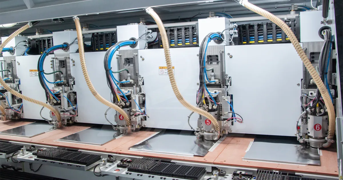
SprintPCB has extensive mass production experience in heavy copper PCBs, especially for new energy, energy storage, and power electronics customers.
Process Capability Table:
| Parameter | Capability Range |
| Outer Layer Copper | 0.5 oz – 6 oz (mass production) |
| Inner Layer Copper | 0.5 oz – 6 oz (mass production) |
| Min. Trace/Space | 2.5mil / 3mil (18 µm), 13mil / 13mil (210 µm) |
| Plated Through-Hole Copper | ≥20 µm |
| Layer Count | 2 – 40 layers |
| Max. Board Thickness | 8.0 mm |
100% AOI optical inspection
Full electrical testing + cross-section analysis
Certified with UL, ISO9001, IATF 16949
Design Review: Free DFM checks for copper thickness, trace width, via plating, and solder mask compatibility.
Prototype Validation: Small batch samples for testing current-carrying and thermal performance.
Cost Optimization: Compare full-board heavy copper with selective heavy copper solutions.
Lead Time Options: Priority scheduling available for urgent projects, ensuring quick ramp-up to mass production.
Heavy copper PCBs are the foundation for high-current and high-reliability products. With SprintPCB's proven expertise in design support, manufacturing capacity, and fast delivery, we have successfully supported hundreds of projects across new energy, energy storage, and industrial power sectors.
Contact SprintPCB today: Share your current, temperature rise, and copper thickness requirements. We will evaluate your design, optimize cost, and provide quick-turn samples—helping your product become more stable, durable, and reliable.

Customer support