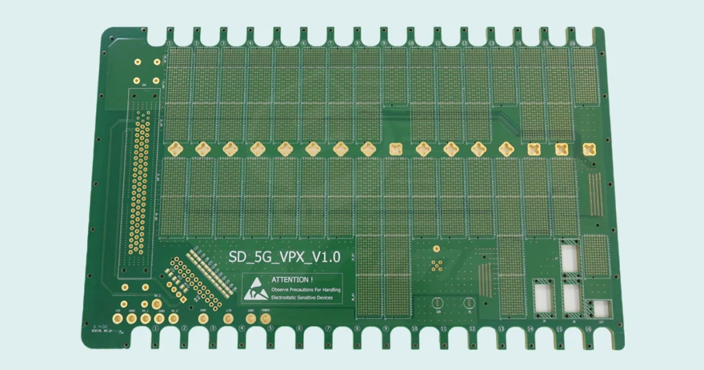
High-Density Interconnect (HDI) PCBs represent a significant advancement in printed circuit board technology, enabling more compact, efficient, and reliable electronic devices. As the demand for miniaturization and high-performance electronics grows, HDI PCBs have become essential in various industries, including consumer electronics, automotive, medical devices, and aerospace. This article explores the intricacies of HDI PCB technology, its advantages, manufacturing processes, and why SprintPCB is your ideal partner for HDI PCB solutions.
Understanding HDI PCB Technology
HDI PCBs are characterized by their higher wiring density per unit area compared to traditional PCBs. They incorporate microvias, blind and buried vias, and fine lines and spaces to achieve superior electrical performance and design flexibility. This technology allows for the integration of more components in a smaller area, leading to lighter and more compact electronic devices.
Advantages of HDI PCBs
HDI PCBs offer numerous benefits over conventional PCBs:
Miniaturization: The use of microvias and fine lines enables the design of smaller and thinner boards, essential for modern compact devices.
Enhanced Electrical Performance: Shorter signal paths reduce signal loss and improve signal integrity, crucial for high-speed applications.
Increased Reliability: The reduced number of interconnections and layers minimizes potential points of failure, enhancing overall reliability.
Design Flexibility: HDI technology supports complex designs with higher component density, allowing for more functionality in a limited space.
Cost-Effective: Despite the advanced technology, HDI PCBs can reduce the overall system cost by minimizing the need for additional components and interconnections.
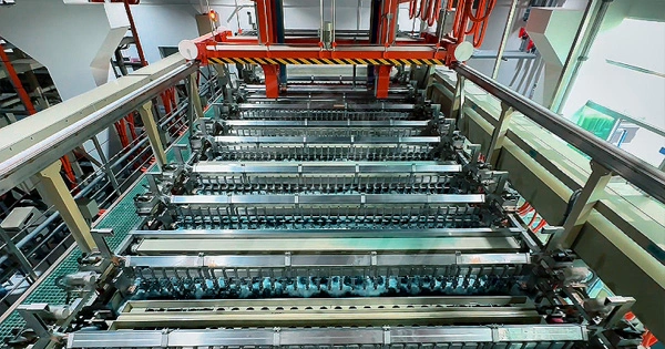
HDI PCB Manufacturing Process
The manufacturing of HDI PCBs involves several specialized processes:
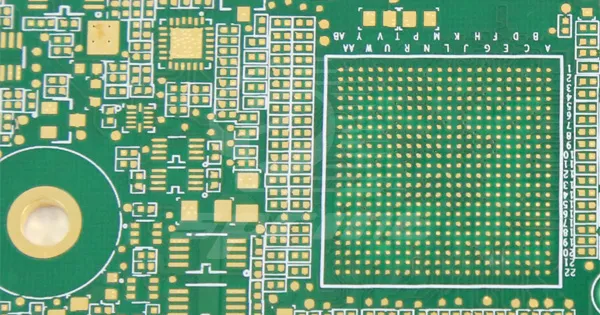
- Laser DrillingHigh-precision laser drilling is used to form microvias—typically less than 0.1 mm in diameter—which enable compact interlayer connections. This process is critical for achieving the fine feature density required in HDI designs.
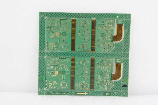
- Blind and Buried ViasBlind vias connect outer layers to one or more inner layers, while buried vias connect only internal layers. These via types are essential in multilayer HDI structures, enabling signal routing without consuming valuable surface space. Complex stack-ups such as 1+N+1 or 2+N+2 are constructed through multiple lamination stages.
- Sequential LaminationHDI PCBs are built layer by layer using sequential lamination. Each cycle includes patterning, via formation (laser drilling), and pressing, allowing for high circuit density and multilayer interconnect structures.
- Via FillingMicrovias and via-in-pad structures are filled with conductive or non-conductive resin to prevent voids, ensure mechanical strength, and create a flat surface for component mounting. This step is especially important for BGA and high-density SMT components.
- Laser Direct Imaging (LDI)Instead of traditional film-based exposure, LDI technology uses a laser to directly expose circuit patterns onto photoresist. This enhances image resolution, improves alignment accuracy, and supports the fine-line features typical of HDI PCBs.
- High-Precision EtchingTraces and spaces on HDI PCBs are often less than 75μm (3 mil). Tightly controlled etching processes are used to ensure dimensional accuracy, edge definition, and uniformity throughout the board.
- Copper PlatingAfter drilling, conductive copper is deposited inside microvias through electroplating to establish reliable electrical connections between layers. Uniform plating thickness is crucial for signal integrity and mechanical strength.
- Impedance ControlStrict control of trace geometry, dielectric materials, and spacing ensures consistent impedance across high-speed signal paths. This is essential for applications requiring signal integrity, such as 5G, automotive radar, and high-frequency computing.
- Surface FinishingFinishes such as ENIG (Electroless Nickel Immersion Gold) are applied to enhance solderability, resist oxidation, and ensure long-term performance. Surface finishing also supports fine-pitch component assembly.
Applications of HDI PCBs
HDI PCBs are integral to various high-performance applications:
- Consumer Electronics: Smartphones, tablets, and wearable devices utilize HDI PCBs for their compact size and high functionality.
- Automotive Systems: Advanced driver-assistance systems (ADAS) and infotainment systems rely on HDI PCBs for reliable performance in compact spaces.
- Medical Devices: Portable medical equipment benefits from the miniaturization and reliability of HDI PCBs.
- Aerospace and Defense: HDI PCBs meet the stringent requirements for reliability and performance in aerospace applications.
Why Choose SprintPCB for HDI PCB Solutions?
SprintPCB stands out as a leading manufacturer of HDI PCBs, offering comprehensive solutions tailored to your specific needs:
- Advanced Technology: Utilizing state-of-the-art equipment, SprintPCB achieves microvia sizes as small as 0.1mm, ensuring high-density interconnections.
- Quality Assurance:Adherence to international standards like ISO 9001 and IATF16949 guarantees the highest quality products.
- Expertise:A team of experienced engineers provides design support and technical guidance throughout the project.
- Customization:SprintPCB offers flexible manufacturing options to accommodate various design requirements and production volumes.
- Global Reach:Serving clients worldwide, SprintPCB ensures timely delivery and responsive customer service.
Conclusion
HDI PCB technology is pivotal in advancing modern electronics, offering unparalleled benefits in miniaturization, performance, and reliability. Partnering with an experienced manufacturer like SprintPCB ensures that your products leverage the full potential of HDI technology. Whether you're developing cutting-edge consumer electronics or critical aerospace systems, SprintPCB provides the expertise and capabilities to meet your HDI PCB needs.