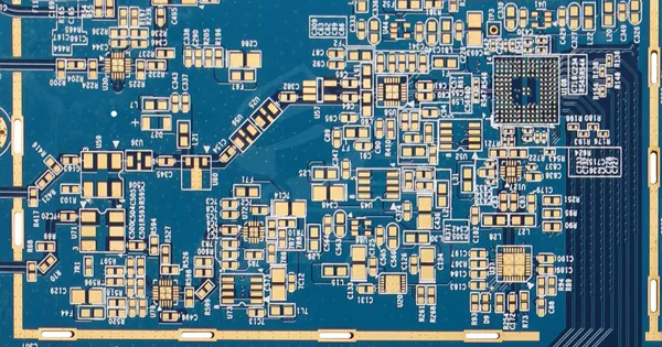
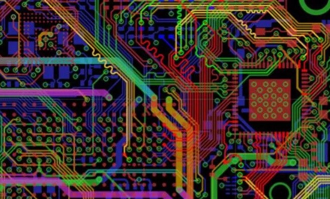
Efficient PCB routing is crucial for the overall performance and reliability of a printed circuit board. Proper routing techniques can help minimize signal noise and interference, reduce crosstalk, and optimize power distribution. In this article, we'll share 10 best practices for PCB routing that can help you design high-quality PCBs.
- Plan ahead and establish a clear routing strategy
Before you start routing your PCB, it's important to plan ahead and establish a clear routing strategy. This includes defining the signal flow, identifying critical components, and deciding on the placement of components. A good routing strategy will help you avoid design errors and minimize the risk of signal integrity issues.
- Use the shortest and most direct routing paths
Short, direct routing paths can help minimize signal delay, reduce crosstalk, and optimize power distribution. When routing, try to keep the traces as straight as possible and avoid using unnecessary vias or bends. Additionally, avoid routing signals near noisy components or high-frequency areas of the board.
- Use differential pairs for high-speed signals
Differential pairs are used to carry high-speed signals with minimal crosstalk and noise. When routing differential pairs, make sure that the length of each trace is equal to ensure balanced impedance. Additionally, keep the traces as close together as possible to minimize electromagnetic interference.
- Group components by function
Grouping components by function can help simplify the routing process and improve signal integrity. For example, grouping all power-related components in one area can help minimize voltage drop and optimize power distribution. Similarly, grouping all signal-related components in one area can help minimize signal noise and interference.
- Route power and ground planes first
When routing a PCB, it's important to start with the power and ground planes first. This ensures that power and ground connections are optimized and reduces the risk of noise and interference. Additionally, this helps to minimize the loop area of the signal traces, reducing the chance of crosstalk.
- Use appropriate trace widths
Trace widths play an important role in the overall performance of a PCB. When routing, use appropriate trace widths based on the current requirements and signal speed. Thicker traces can handle higher currents, while thinner traces can help reduce parasitic capacitance and optimize high-speed signals.
- Minimize the use of vias
Vias can introduce noise and signal delay, and they can also increase the overall cost of the PCB. When routing, try to minimize the use of vias and use them only when necessary. Additionally, avoid using blind or buried vias, which can be more expensive and difficult to manufacture.
- Use teardrops for high-density designs
Teardrops are used to maintain the integrity of the copper trace when it transitions to a via or pad. In high-density designs, teardrops can help reduce the risk of breakage and ensure the reliability of the PCB. When using teardrops, make sure to maintain a sufficient distance between the trace and the via or pad to prevent short circuits.
- Test and validate your design
After completing your PCB routing, it's important to test and validate your design to ensure that it meets the required specifications. Use simulation and analysis tools to test the signal integrity, power distribution, and thermal performance of the PCB. Additionally, perform a design rule check (DRC) to identify and fix any errors or inconsistencies.
- Stay up-to-date with the latest routing techniques
PCB routing techniques are constantly evolving, and it's important to stay up-to-date with the latest best practices and trends. Join online forums, attend webinars and workshops, and read industry publications to stay informed and learn