As electronic devices evolve toward higher functionality and miniaturization, multilayer PCB assembly has become an industry standard for advanced applications. From consumer electronics to medical devices, automotive systems, and aerospace technology, multilayer printed circuit boards are critical for achieving high density, performance, and reliability in compact form factors. This article SprintPCB explores the processes of multilayer PCB assembly involved.

Multilayer PCB assembly is the process of fabricating and assembling printed circuit boards that contain three or more conductive copper layers. These layers are separated by insulating dielectric materials, laminated under heat and pressure, and interconnected through vias. The result is a highly compact yet powerful circuit board that can handle complex functions without increasing the overall board size.
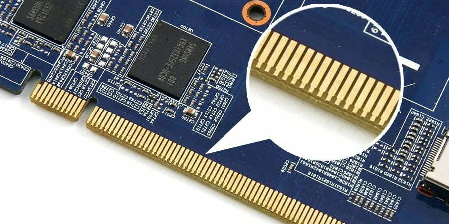
Compared with single- or double-sided PCBs, multilayer PCB assembly allows engineers to design advanced circuits within a smaller footprint. This makes multilayer boards indispensable in modern electronics where space is limited but performance demands are high, such as smartphones, servers, and medical devices. In addition to supporting high-speed signals, they also provide enhanced reliability, making them a preferred choice for industries that require precision and durability.
Producing reliable multilayer PCB assemblies involves multiple stages, each requiring strict precision and quality control. From raw materials to final testing, every step plays a role in ensuring that the finished boards perform as expected in demanding environments.
The first step in multilayer PCB assembly is fabricating the bare multilayer board. Copper and dielectric layers are stacked and laminated under controlled conditions. Vias are drilled to connect internal and external layers. Precision at this stage is critical, because even a slight misalignment can affect the performance of all subsequent layers. High-quality fabrication ensures signal accuracy, reduced noise, and overall board stability.
Before components can be mounted, solder paste is applied to the PCB pads. SprintPCB and other leading manufacturers use laser-cut stencils to ensure paste is deposited precisely where needed. This step reduces soldering defects and ensures consistent joints, which is especially important in multilayer PCB assembly, where dense layouts and fine-pitch components leave little margin for error.
Both surface-mount technology (SMT) and through-hole technology (THT) are commonly used in multilayer PCB assembly. Advanced pick-and-place machines can accurately position hundreds of components per minute, including fine-pitch ICs and BGAs. For components requiring higher mechanical strength, THT soldering is applied. This flexibility allows multilayer PCBs to accommodate both high-density digital ICs and robust connectors.
Once components are placed, soldering is performed. SMT components typically go through reflow soldering, where controlled heat melts the solder paste and secures the parts. THT components may undergo wave soldering or selective soldering. In multilayer PCB assembly, precise temperature control is essential to prevent cold joints, solder bridging, or damage to sensitive components.
The final stage of multilayer PCB assembly is rigorous inspection and testing to ensure flawless performance. This includes:
AOI (Automated Optical Inspection): Detects solder defects and placement errors.
X-ray Inspection: Identifies hidden solder joints under BGAs and QFNs.
ICT (In-Circuit Testing): Verifies electrical connections and component values.
Functional Testing: Simulates real-world operation to ensure reliability.
Together, these steps guarantee that every multilayer PCB delivered to the customer meets the highest industry standards.
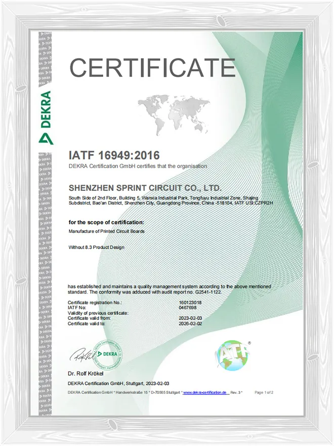
When it comes to selecting a reliable partner, SprintPCB stands out with its strong PCB manufacturing base and comprehensive assembly services. Unlike providers who outsource part of the process, SprintPCB handles every stage in-house, ensuring quality, efficiency, and shorter lead times.
Key services include:
PCB Manufacturing: In-house production ensures consistency and fast turnaround.
Stencil Production: Custom laser-cut stencils for accurate solder paste application.
Component Sourcing: Global procurement with cost control and authenticity guarantees.
Assembly Services: SMT, THT, mixed technology, BGA, and fine-pitch assembly for multilayer PCBs.
IC Programming: On-board programming across major platforms.
PCBA Testing: AOI, ICT, functional tests, and advanced X-ray inspection.
Prototyping & Batch Production: From single-piece prototypes to scalable large-volume runs.
Turnkey Solutions: Complete management of manufacturing, sourcing, and assembly.
By keeping all steps under one roof, SprintPCB reduces risks, eliminates delays, and ensures that every multilayer PCB assembly project is delivered with precision and reliability. This makes them a trusted partner for businesses across industries, whether for prototype development or full-scale production.
Multilayer PCB assembly is at the core of today's electronics industry, enabling compact, high-performance, and reliable designs. Each step—fabrication, soldering, placement, and testing—must be executed with accuracy to ensure final product quality.
While many providers offer PCB assembly services, companies like SprintPCB bring added value by integrating PCB manufacturing, component sourcing, assembly, and testing under one streamlined process. This one-stop approach not only improves efficiency but also gives customers peace of mind, knowing that their projects will be delivered on time and with uncompromised quality.
For businesses looking to bring designs from concept to reality, choosing the right partner for multilayer PCB assembly can make all the difference.

Customer support