A Printed Circuit Board (PCB) is a crucial component in electronic devices. Serving as a platform to connect and support electronic components, the quality and performance of PCBs significantly impact the reliability and functionality of the devices. As one of the key steps in PCB manufacturing, surface treatment plays a vital role in ensuring the quality and reliability of PCBs.
This article will focus on discussing the PCB surface treatment thickness and its relationship with IPC (Institute for Printed Circuits) standards. The surface treatment thickness refers to the thickness of the surface treatment layer, which is crucial for the performance, reliability, and lifespan of PCBs. Ensuring that the surface treatment thickness meets the requirements of IPC standards is essential for ensuring product quality and consistency during the manufacturing process.
In the following article, we will delve into different surface treatment methods and the requirements of IPC standards regarding PCB surface treatment thickness. We will explain the working principles, advantages, and application scenarios of each surface treatment method, as well as provide a detailed overview of the IPC standards governing PCB surface treatment thickness.
Additionally, we will offer practical recommendations to assist manufacturers in implementing and controlling PCB surface treatment thickness in practice, ensuring product quality and performance.
The Basic Concept of PCB Surface Treatment.
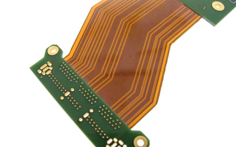
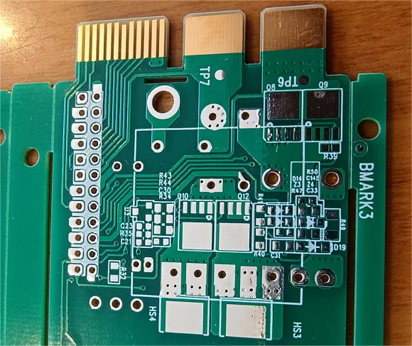
PCB surface treatment is a process of applying a layer of specific material on the surface of a printed circuit board to provide protection, enhance conductivity, prevent corrosion, or improve solderability. In the PCB manufacturing process, common surface treatment methods include immersion gold, immersion silver, immersion tin, and ENEPIG (Electroless Nickel Electroless Palladium Immersion Gold).
Electroless Nickel Immersion Gold (ENIG):
ENIG is a method of depositing a layer of gold onto the surface of a PCB through electroless plating. It utilizes an electrochemical process to create a metallic protective layer on the PCB surface. ENIG offers excellent conductivity and corrosion resistance, making it a preferred choice for high-performance applications. ENIG also exhibits good solderability, as gold is a highly solderable metal.
Electroless Silver (ES):
Electroless Silver is a method of depositing a silver metal layer on the surface of a PCB through electroless plating. It forms a thin film of silver on the PCB surface. It exhibits good conductivity and thermal conductivity, and it is cost-effective, making it an alternative in certain applications. Electroless Silver is typically used in high-frequency circuits or high-power applications.
Hot Air Solder Leveling (HASL):
HASL, also known as Hot Air Solder Leveling, is a commonly used surface treatment method. It involves applying a layer of tin onto the surface of a PCB and using hot air to melt and spread it.
ENEPIG (Electroless Nickel Electroless Palladium Immersion Gold):
ENEPIG (Electroless Nickel Electroless Palladium Immersion Gold) is a high-performance surface treatment method where a composite thin film of nickel, palladium, and gold is sequentially deposited on the surface of a PCB. The IPC-4556 standard also covers the requirements for ENEPIG, including the thickness of nickel, palladium, and gold, as well as properties such as heat resistance, corrosion resistance, and solderability.
In practice, manufacturers need to choose the appropriate surface treatment method based on specific applications and requirements, and tightly control the thickness of the surface treatment to ensure the performance and reliability of PCBs. This involves using proper process parameters and quality control measures, such as accurate material measurement and inspection methods, to ensure compliance with IPC standards.
The Importance of PCB Surface Treatment Thickness
The thickness of PCB surface treatment plays a crucial role in soldering reliability, electrical performance, corrosion resistance, soldering process capability, and compatibility.
The thickness of PCB surface treatment is essential for soldering reliability. Surface treatment layers such as immersion gold, immersion silver, and immersion tin provide a good soldering surface, enabling proper wetting of solder and the formation of uniform solder joints.
The appropriate thickness of surface treatment ensures the quality of solder joints, prevents soldering defects such as solder peel-off and incomplete filling of solder joints, thus improving the soldering reliability of the PCB.
The surface treatment thickness of PCB is also crucial for electrical performance. Different surface treatment methods possess varied resistivity and conductivity characteristics. By controlling the surface treatment thickness, it is possible to ensure that the resistance values and conductivity characteristics fall within the required design range, thereby maintaining the normal functionality and performance of the circuit.
The PCB surface treatment layer can provide a protective barrier, preventing the metal traces and pads of the PCB from reacting with oxygen, moisture, chemicals, and other elements in the environment. The appropriate thickness of the surface treatment layer can effectively enhance the corrosion resistance of the PCB and prolong its lifespan.
The surface treatment layer can enhance the soldering process performance of PCBs. For example, immersion gold surface treatment offers excellent solderability and oxidation resistance, making the soldering process more stable and controllable. Appropriate surface treatment thickness can provide suitable soldering conditions and process windows, thereby reducing the occurrence of soldering defects and improving production efficiency.
Different electronic components and devices may have specific requirements for PCB surface treatment thickness. Following IPC (Institute for Printed Circuits) standards and industry specifications to ensure that the PCB surface treatment thickness meets the compatibility requirements of components and devices contributes to the overall system stability and performance.
By achieving appropriate surface treatment thickness, the quality, reliability, and performance of PCBs can be improved, while reducing welding defects and quality issues in production. Therefore, strict control and adherence to IPC standards regarding surface treatment thickness requirements are crucial in the PCB manufacturing and design processes.
IPC Standards for PCB Surface Treatment Thickness
IPC (Institute for Printed Circuits) standards are a widely used series of standards in the electronics industry, governing various aspects of the printed circuit board (PCB) manufacturing process. Below, we will provide a detailed description of the specific requirements and measurement methods outlined in IPC-4552A standard (Immersion Gold), IPC-4553 standard (Immersion Silver), IPC-4554 standard (Immersion Tin), and IPC-4556 standard (Electroless Nickel Electroless Palladium Immersion Gold, or ENEPIG).
IPC-4552A Standard (Immersion Gold):
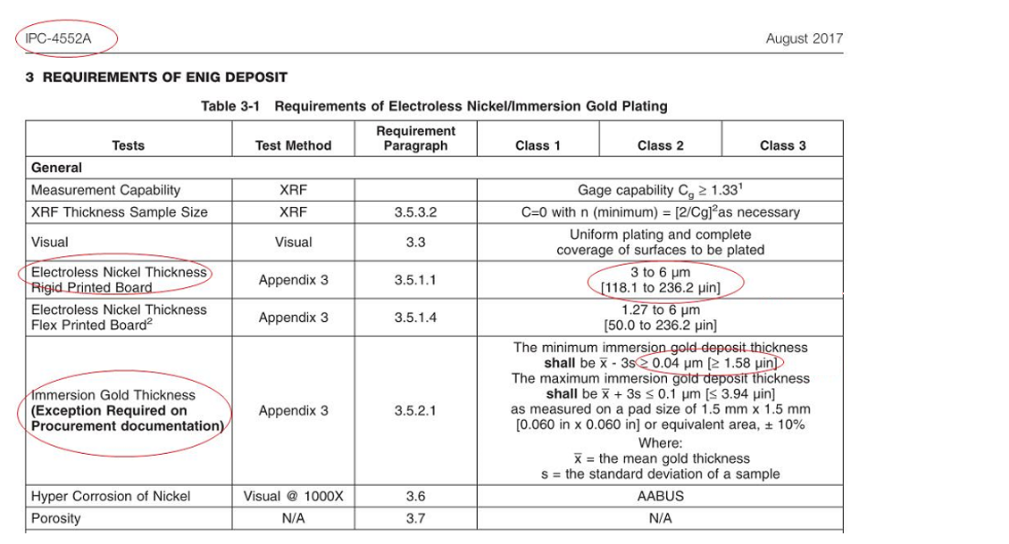
The IPC-4552A standard specifies the requirements and specifications for the immersion gold surface treatment. It requires a minimum thickness of 1.58U for the immersion gold layer, although the industry typically follows a thickness standard of 2U. The standard also specifies the coating performance, heat resistance, corrosion resistance, and other requirements for the immersion gold layer, with a nickel thickness of 3-6μm.
The measurement methods include using X-ray fluorescence spectroscopy (XRF) to measure the metal thickness and examining and measuring the uniformity and coverage of the coating by stripping the coating from the sample and inspecting it under a microscope.
IPC-4553 Standard (Immersion Silver):
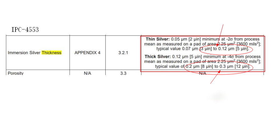
The IPC-4553 standard defines the requirements and specifications for the immersion silver surface treatment. The thickness of the immersion silver layer is categorized into thin silver and thick silver. The thickness of thin silver should be within the range of 3 to 5U. The thickness of thick silver should be within the range of 8 to 12U, which is commonly adopted in the industry.
IPC-4554 Standard (Immersion Tin):
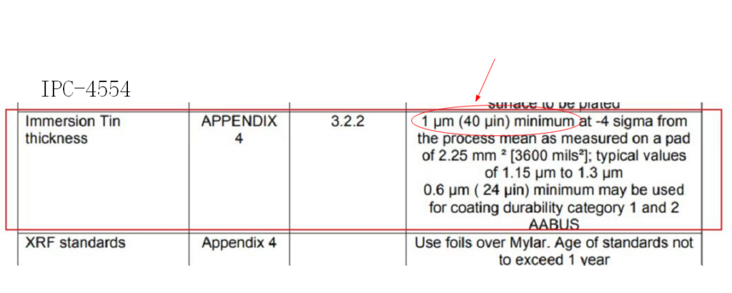
The IPC-4554 standard specifies the requirements and specifications for Immersion Tin surface treatment.
The standard requires a typical thickness of the Immersion Tin layer to be around 1 μm.
It also specifies requirements for the coating performance, heat resistance, corrosion resistance, and other aspects of the Immersion Tin layer.
Measurement methods include using X-ray Fluorescence Spectrometry (XRF) to measure the metal thickness and inspecting and measuring the uniformity and coverage of the coating by stripping the layer from the sample and examining it under a microscope.
Please note that while I have translated the information provided to the best of my abilities, it's always a good idea to consult the official IPC-4554 standard for accurate and detailed information.
IPC-4556 Standard (ENEPIG):
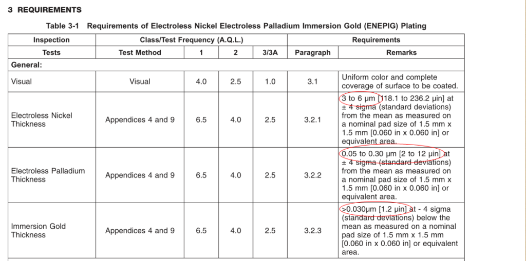
The IPC-4556 standard defines the requirements and specifications for ENEPIG (Electroless Nickel Electroless Palladium Immersion Gold) surface treatment.
The standard mandates that the nickel layer thickness for ENEPIG should be between 3 and 6μm, the palladium layer thickness should be between 2 and 12U, and the gold layer thickness should be equal to or greater than 1.2μm.
The standards also specify requirements for the coating performance, heat resistance, and corrosion resistance of the ENEPIG layer.
Measurement methods include using X-ray fluorescence spectroscopy (XRF) to measure the thickness of the nickel, palladium, and gold layers, as well as stripping the coating from the sample and using microscopy to inspect and measure the uniformity and coverage of the coating.
These requirements and measurement methods specified by the IPC standards aim to ensure the quality, consistency, and reliability of the PCB surface treatment layers. By adhering to these standards, manufacturers can ensure that the PCB surface treatment thickness complies with industry standards and meets the performance and reliability requirements of the PCB.
How to Implement and Control PCB Surface Treatment Thickness in Practice
Process Control:
During the PCB manufacturing process, it is important to strictly adhere to the correct process parameters and workflow during the surface treatment stage. This includes controlling the concentration, temperature, pH value, and processing time of chemical solutions.
For different surface treatment methods, refer to the guidelines provided by suppliers or relevant standards to ensure the correct process parameters and steps are followed to achieve the desired surface treatment thickness.
Detection and Measurement:
Utilize appropriate measurement tools and equipment to detect and measure the PCB surface treatment thickness. Common measurement methods include X-ray fluorescence (XRF) measurement instruments, scanning electron microscopes (SEM), and ion chromatography (ICP), among others.
Ensure the accuracy and calibration of the measurement equipment to obtain reliable and consistent measurement results.
Technical Requirements and Standards:
Refer to IPC standards or relevant industry standards to understand the technical requirements and specifications for surface treatment thickness. For example, the IPC-4552A standard is used for immersion gold, IPC-4553 for immersion silver, IPC-4554 for immersion tin, and IPC-4556 for ENEPIG. By following these standards and adopting their recommended measurement methods and requirements, ensure that the surface treatment thickness meets the specified requirements of the standards.
Process Control and Documentation:
During the manufacturing process, implement process control and documentation to ensure the consistency and traceability of surface treatment thickness.
Record process parameters, measurement results, and inspection data, and establish process control charts or data analysis to monitor and control variations in surface treatment thickness. Take corrective measures promptly when necessary.
Training and Quality Management:
Provide necessary training and guidance to operators to ensure their understanding of surface treatment methods, process parameters, and control requirements.
Implement an effective quality management system, including internal audits and continuous improvement, to ensure that surface treatment thickness meets quality standards and to rectify any potential issues or deviations.
Supplier Selection and Collaboration:
Selecting reliable suppliers and partnering with them is crucial. Look for suppliers with experience and expertise in providing surface treatment services that meet your requirements.
Collaborate closely with your suppliers to ensure they understand and fulfill your surface treatment thickness requirements. Establishing a stable supply chain is essential in maintaining consistent quality.
In this article, we have discussed the relationship between PCB surface treatment thickness and IPC standards. By gaining a deeper understanding of commonly used surface treatment methods such as immersion gold, immersion silver, immersion tin, and ENEPIG, we have realized the critical importance of proper surface treatment thickness in ensuring the quality and performance of PCBs.
Adhering to IPC standards is key to ensuring the consistency and compliance of PCB surface treatment thickness. In conclusion, understanding IPC standards and implementing appropriate control measures are crucial in ensuring that PCB surface treatment thickness meets the requirements of IPC standards. Only then can we achieve high-quality, reliable printed circuit boards that meet the demands of various application fields.
SprintPCB: Your Reliable PCB Support Provider SprintPCB is a renowned high-tech enterprise offering comprehensive PCB manufacturing services to clients globally. With our extensive expertise and cost-effective solutions, you can prioritize your organization's critical requirements while enjoying a seamless process. Get in touch with us today and discover how we can assist you.