PCB Impedance Test Coupons are specially designed structures on a PCB used to measure and validate the impedance characteristics of the PCB's transmission lines. Impedance is a crucial parameter in high-speed digital and analog circuits, as it determines the signal integrity and performance of the PCB.
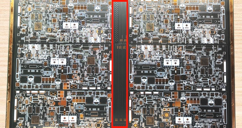
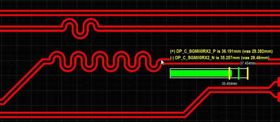
During the PCB manufacturing process, impedance test coupons are fabricated alongside the main PCB. They should be strategically located on the same PCB panel as the main PCB, usually in the middle of the working panel. They undergo the same fabrication steps, including etching, plating, and solder mask application. However, additional measurements and tests are performed on these coupons to verify the impedance characteristics. Impedance test coupons are commonly used to test PCBs in the field of high-frequency electronics, such as communication devices, radio frequency circuits, radar systems, and high-speed data transmission. These coupons assist in verifying whether the impedance characteristics of the PCB meet the design requirements, ensuring the quality of signal transmission and impedance matching performance. There is a close relationship between impedance test coupons and trace width and spacing. When designing impedance test coupons, specific trace width and spacing are typically used to achieve the desired impedance value. According to the characteristic impedance formula for transmission lines, increasing the trace width decreases the line's resistance, resulting in a lower impedance value, and vice versa. Therefore, by adjusting the combination of trace width and spacing, the desired impedance value can be achieved. The commonly used characteristic impedance formulas are as follows:
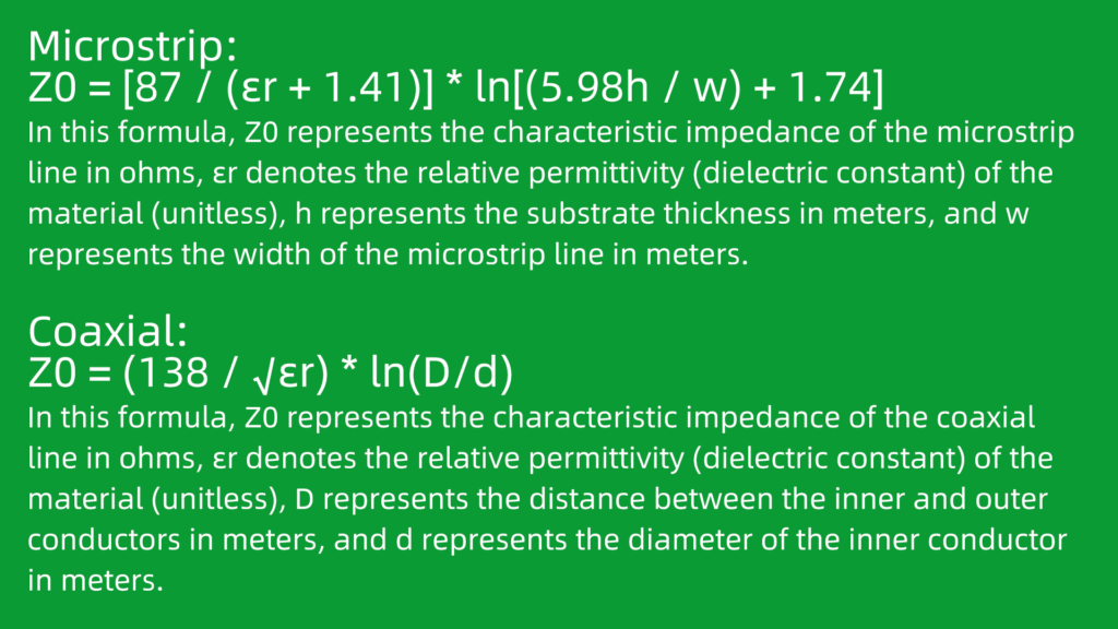
Microstrip: Z0 = [87 / (εr + 1.41)] * ln [(5.98h / w) + 1.74] In this formula, Z0 represents the characteristic impedance of the microstrip line in ohms, εr denotes the relative permittivity (dielectric constant) of the material (unitless), h represents the substrate thickness in meters, and w represents the width of the microstrip line in meters. Coaxial: Z0 = (138 / √εr) * ln(D/d) In this formula, Z0 represents the characteristic impedance of the coaxial line in ohms, εr denotes the relative permittivity (dielectric constant) of the material (unitless), D represents the distance between the inner and outer conductors in meters, and d represents the diameter of the inner conductor in meters. While test coupons help identify manufacturing defects and reduce debugging and redesign costs, they have limitations. Using PCB test coupons can impact costs by increasing labor expenses and reducing board material utilization, thus increasing raw material costs. In the PCB manufacturing process, test coupons typically require separate design, fabrication, and assembly, which means additional labor and time are needed to handle them. Additionally, test coupons often occupy a portion of the PCB board space, reducing overall board material utilization and resulting in additional raw material costs.

Customer support