In the field of electronic manufacturing, printed circuit boards (PCBs) are essential foundational components that play a crucial role in connecting and supporting electronic elements. However, to ensure the performance and reliability of PCBs, surface treatment processes are of paramount importance. Among numerous surface treatment techniques, today we will focus on 'Electroless Nickel Immersion Gold (ENIG)' and explore its mysteries, advantages, and challenges in PCB manufacturing.
Electroplating Process of Immersion Gold
The immersion gold process, also known as immersion nickel-gold or chemical nickel-gold, is renowned for its unique characteristics and wide range of applications.
In this process, a layer of nickel with an appropriate thickness is first deposited on the surface conductor of the PCB through chemical methods. Subsequently, a layer of gold with a specific thickness (usually 0.025-0.075 micrometers) is deposited onto the nickel layer.
This procedure not only imparts excellent flatness to the surface of the solder pad but also forms a protective layer on the surface and sides. This not only aids in soldering but also enables various forms of bonding or wire bonding, thus providing greater possibilities for the connection of electronic components.
Advantages of Electroless Nickel Immersion Gold (ENIG): Flatness and Versatility
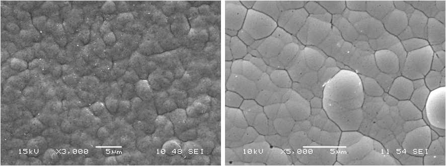
The Electroless Nickel Immersion Gold (ENIG) process stands out in PCB manufacturing due to its excellent flatness and versatility. The flatness of the solder pad surface is a crucial factor in ensuring stable connectivity and performance of electronic components.
Moreover, a flat solder pad surface helps reduce soldering stress and enhances the reliability of electronic products. The ENIG process employs precise chemical methods to uniformly deposit layers of nickel and gold onto the solder pad surface, resulting in a smooth and flat finish.
The flatness of the solder pad surface is crucial for various types of connections, especially in the manufacturing of microelectronic devices and high-density integrated circuits. Whether it's traditional soldering, more complex bump bonding, or wire bonding, the ENIG (Electroless Nickel Immersion Gold) process provides an ideal foundation for these connection methods.
During welding, a flat surface ensures even distribution of solder, resulting in more reliable solder joints and connections. In overlap welding or metal wire welding, the smoothness of the solder mask provides a stable support platform for the wire, ensuring precise positioning of solder joints and high-quality connections.
In addition, the immersion gold layer, as a superior protective coating, can form a robust barrier on the surface and sides of the solder pad, effectively isolating it from external oxygen, humidity, and chemical substances. This not only extends the lifespan of the solder pad but also enhances the stability and reliability of the components.
In extreme environments such as high temperature, high humidity, or corrosive gas environments, the protective role of the immersion gold layer is particularly remarkable, providing electronic components with a strong resistance capability.
The immersion gold process not only enhances the flatness of the solder pads, improving soldering quality and connection stability, but also provides greater application flexibility for PCBs. Whether using traditional soldering methods or more advanced connection techniques, the immersion gold process can offer a solid foundation, enabling excellent performance in various fields.
Challenges Faced by Immersion Gold
While immersion gold technology indeed offers numerous advantages in PCB manufacturing, it also comes with a series of challenges.
Complexity of Craftsmanship
The intricate and intricate manufacturing process. The complexity of the electroplating process arises from several key steps in its manufacturing.
Firstly, the deposition of nickel requires strict control of parameters such as temperature, concentration, and current to ensure the uniformity and compactness of the nickel layer.
Subsequently, the replacement of the gold layer demands precise control of time and concentration to avoid excessive or insufficient gold layer thickness. The meticulous requirements of these steps make the manufacturing process intricate, necessitating highly specialized equipment and technical support, thereby increasing the difficulty and complexity of manufacturing.
Cost Considerations
High manufacturing costs. The complexity of the electroplating process directly results in an increase in manufacturing costs.
To ensure that each step meets the standards, manufacturers need to invest significant amounts of labor, equipment, and time. The demands for precise control also imply greater investments in equipment maintenance and calibration.
Additionally, the expensive materials required for the electroplating process, such as gold and nickel salts, also exert certain pressures on manufacturing costs. Therefore, while the electroplating process can provide high-quality PCB surface treatment, its high manufacturing costs limit its widespread application in certain contexts.
Underplating and Penetrating Plating Issues
Potential Risks in Manufacturing Defects.
Under specific conditions, the electroplating process may encounter problems of underplating and penetrating plating, which can lead to severe defects in PCB manufacturing.
Underplating refers to the incomplete deposition of sufficient nickel or gold layers on the PCB conductor surface, resulting in unstable or even failed connections of electronic components.
On the other hand, penetrating plating involves the infiltration of metal ions into non-conductive areas, potentially leading to circuit shorts or other issues. The occurrence of these problems could introduce greater uncertainty in the manufacturing process, necessitating more stringent quality control and detection methods to prevent potential defects.
Phosphorus Content in Nickel Plating
Considerations for Special Applications.
In the nickel-plating process, the nickel layer contains 6-9% phosphorus, which may raise certain concerns for specific applications.
For instance, in some high-frequency circuits, the presence of phosphorus could potentially interfere with signal transmission. Additionally, for applications with strict material composition requirements, the presence of phosphorus might limit the suitability of the nickel-plating process. Therefore, when selecting a surface treatment process, manufacturers need to balance the impact of phosphorus content on the final product performance.
Despite facing these challenges in PCB manufacturing, the immersion gold process is expected to gradually overcome these issues with the continuous advancement of technology and ongoing process optimization.
In the future, with the introduction of new materials, new technologies, and improvements in the manufacturing process, the immersion gold process is poised to enhance its reliability and applicability, bringing greater opportunities for development to the electronics manufacturing industry.
Black Pad Effect: Deciphering the Nickel Passivation Phenomenon
In the PCB manufacturing process within the realm of electronics, the electroless nickel process, as a facet of surface treatment, provides an ideal platform for soldering and connectivity.
However, just like in many common cases of technological applications, the process of electroless nickel plating is not without flaws. One of the notable concerns is the "black spot effect," a mysterious phenomenon directly related to the reliability and stability of the process.
The black pad effect refers to a phenomenon of nickel passivation, primarily occurring at the interface between nickel and gold.
In simple terms, this occurs because the nickel layer can undergo excessive oxidation under certain conditions, forming a dense layer of nickel oxide film, resulting in a black appearance on the solder pad surface. This could have significant implications for PCB manufacturing and component connections, such as compromised component adhesion to the solder pad, decreased solder joint quality, and even potential issues with component detachment.
The mechanism of the black disk effect is unusually complex, involving interactions between various chemical and physical processes.
Scientists have discovered during their research that there are numerous factors influencing the black disk effect, including the thickness of the nickel layer, the morphology of the metal junction interface, and the differences in crystal structures between nickel and gold. Additionally, process parameters and environmental conditions may also have an impact on the black disk effect.
Despite the complex mechanisms of the black pad effect, this challenging issue has sparked strong interest among researchers, driving their continuous exploration in the field of PCB surface treatment. Through in-depth research, scientists are diligently seeking stable and reliable solutions to mitigate or eliminate the impact of the black pad effect.
Over the past decades, researchers have proposed numerous methods to address the black pad effect, such as optimizing the fabrication process of nickel layers, adjusting the structure of metal interfaces, and even exploring new alloy materials. These efforts have not only contributed to enhancing the reliability of PCB manufacturing but have also opened up new possibilities for advancements in the field of electronics.
As an integral part of PCB surface treatment, the immersion gold process plays an indispensable role in the field of electronics. It provides a smooth solder pad surface for the connection of electronic components and plays a crucial role in protecting components from oxidation and corrosion.
However, the complex process and challenging issues also require us to continuously explore and innovate to ensure the reliability and stability of the electronics industry. Through a deep understanding of the immersion gold process, we can better comprehend the science and technology behind PCB manufacturing and contribute a modest effort to the development of the electronics sector.
Enhance Your PCB Manufacturing with
SprintPCBSprintPCB is a leading high-tech company that offers top-notch PCB manufacturing services to clients worldwide. With our wealth of industry expertise and cost-effective solutions, you can concentrate on the core aspects of your business. Reach out to us now to explore the possibilities of collaboration and witness the realization of your objectives.