In the modern field of electronics, as device sizes continue to shrink and performance keeps improving, thermal management issues have become increasingly prominent and cannot be ignored. Just as a wise person once said, "Technological advancement often comes hand in hand with the release of heat." The heat generated by electronic devices during operation, if not properly dealt with and dissipated, can be like an imperceptible threat, quietly endangering the stability and lifespan of the equipment. In this ever-changing digital world, mastering key techniques for PCB (Printed Circuit Board) cooling is not only a guarantee for enhancing the reliability of electronic devices but also an essential path toward leading the forefront of technology.
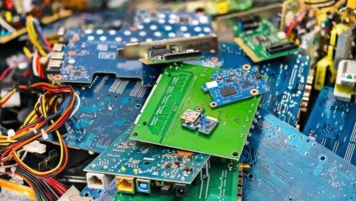
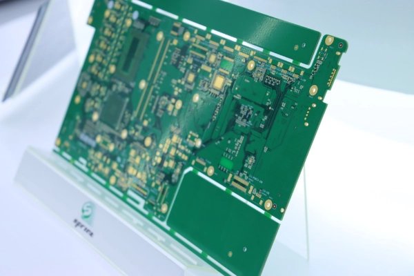
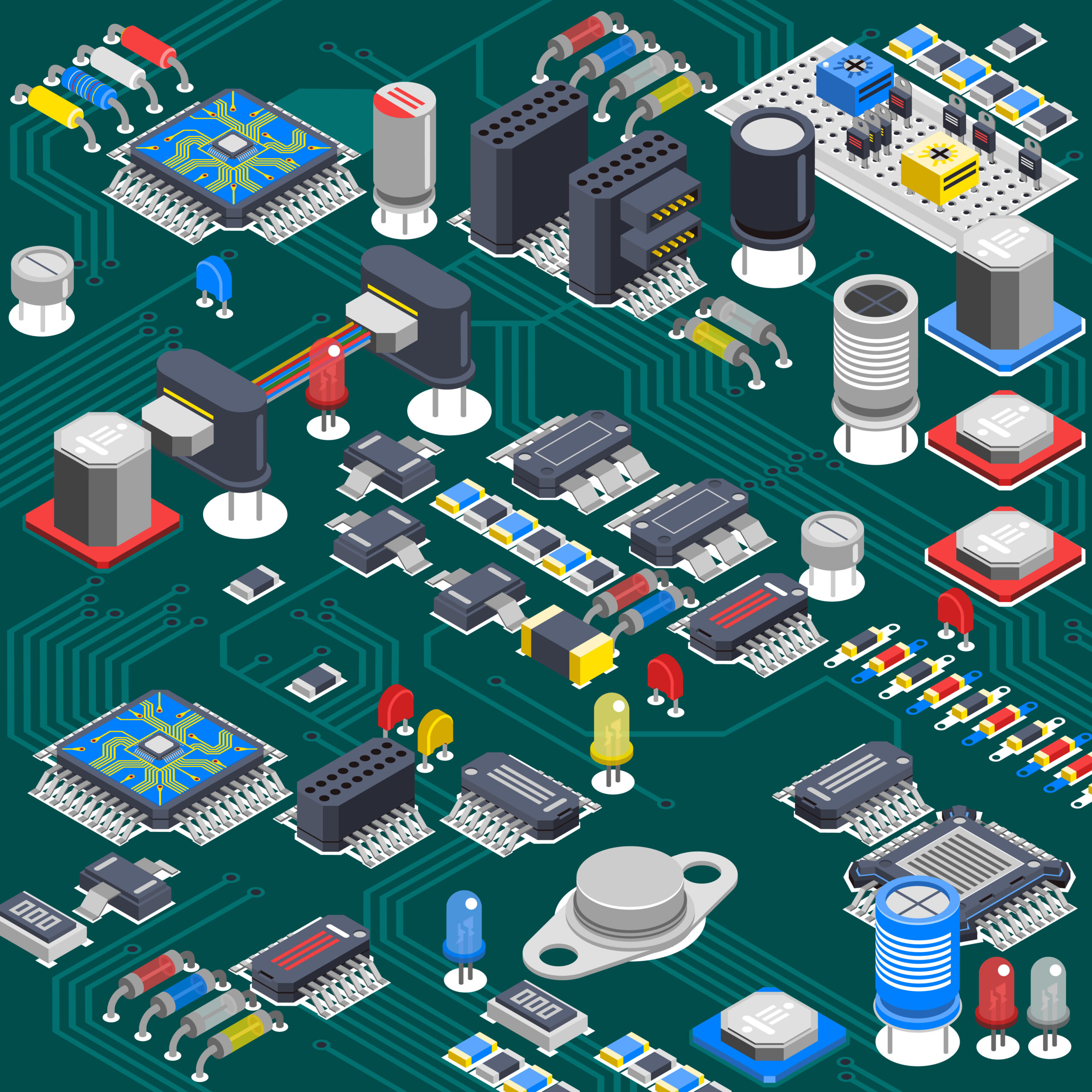
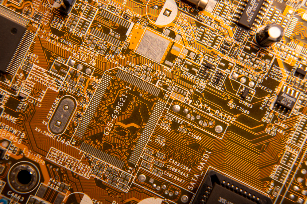
Electronic devices generate a certain amount of heat during operation, causing the internal temperature of the device to rise rapidly. If this heat is not promptly dissipated, the device will continue to heat up, leading to component failure due to overheating, thereby reducing the reliability and performance of the electronic device. Therefore, it is crucial to effectively manage the heat dissipation of the circuit board. Heat dissipation for PCBs plays a vital role, so let's discuss some techniques for PCB heat dissipation. The widely used PCB materials for heat dissipation include copper-clad epoxy glass cloth substrate or phenolic resin glass cloth substrate, with a small number also utilizing paper-based copper-clad boards. While these substrates possess excellent electrical and processing properties, their heat dissipation is poor. As a cooling method for high-heat-generating components, it is nearly impossible to rely on thermal conduction through the PCB resin itself, but rather, heat is dissipated from the surface of the components into the surrounding air. But with the advent of electronic products entering the era of miniaturized components, high-density assembly, and high heat generation, relying solely on the small surface area of components for heat dissipation is far from sufficient. Simultaneously, due to the widespread use of surface-mounted components such as QFP and BGA, the heat generated by electronic components is extensively transferred to the PCB. Therefore, the most effective method to address heat dissipation is to enhance the PCB's inherent heat dissipation capability in direct contact with the heat-generating components, allowing for conduction or dissipation of heat through the PCB.
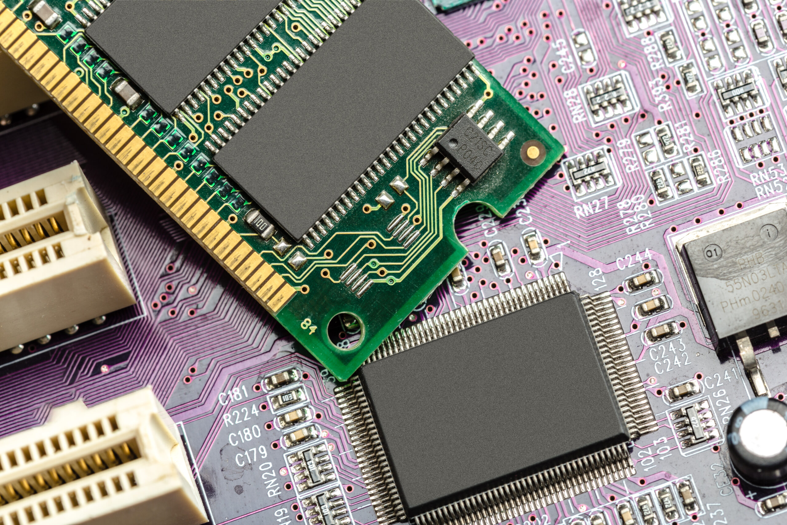
For equipment utilizing free convection air cooling, it is preferable to arrange integrated circuits (or other components) in a vertical orientation or a horizontal orientation. To achieve efficient heat dissipation through a well-designed routing scheme, enhancing copper trace retention and incorporating thermal vias are the primary methods. Due to the poor thermal conductivity of resin within the board material, copper traces and vias serve as effective conductors of heat. Evaluating a PCB's heat dissipation capability necessitates the calculation of the equivalent thermal conductivity of the composite material, which comprises various materials with differing thermal conductivities, used in the PCB's insulating substrate. Components on the same printed circuit board should be arranged into zones based on their heat generation and heat dissipation capabilities. Components with lower heat generation or lower heat resistance, such as small-signal transistors, small-scale integrated circuits, and electrolytic capacitors, should be placed upstream of the cooling airflow (inlet). Components with higher heat generation or better heat resistance, such as power transistors and large-scale integrated circuits, should be placed downstream of the cooling airflow. In the horizontal direction, high-power devices should be arranged closer to the edge of the printed circuit board to shorten the heat transfer path. In the vertical direction, high-power devices should be positioned above on the printed circuit board to minimize their impact on the temperatures of other components. The heat dissipation of the printed circuit board inside the device primarily relies on the flow of air. Therefore, during the design phase, it is crucial to study the airflow pathways and strategically position components or the printed circuit board. Air tends to flow towards areas of lower resistance when in motion, so when placing components on a printed circuit board, it is important to avoid leaving large voids in a particular area. The configuration of multiple printed circuit boards within the assembly should also take into consideration the same issues. It is advisable to place temperature-sensitive components in the lowest temperature zone (such as the bottom of the device). Avoid placing them directly above heat-emitting components. When dealing with multiple components, it is preferable to arrange them in an interleaved layout on a horizontal plane. Place the components with the highest power consumption and maximum heat generation near the optimal heat dissipation location. Avoid placing high-heat generating components in the corners and edges of the printed circuit board unless there are heat dissipation devices arranged nearby. When designing power resistors, choose larger components whenever possible, and ensure sufficient heat dissipation space when adjusting the printed circuit board layout. Minimize the concentration of hotspots on the PCB and distribute the power as evenly as possible across the PCB to maintain uniform and consistent surface temperature performance. Achieving a strict uniform distribution is often challenging in the design process, but it is essential to avoid regions with excessively high-power density. This precaution is taken to prevent the occurrence of hotspots that could adversely affect the normal operation of the circuit. Performing thermal energy analysis for printed circuits is essential if conditions allow for it. The inclusion of thermal energy index analysis software modules in some professional PCB design software nowadays can assist design engineers in optimizing circuit design. In the modern high-tech field, the significance of PCB thermal management techniques is becoming increasingly prominent. Just as a great architect must consider the stability of a skyscraper when designing it, electronic engineers must also focus on the flow and dispersion of heat when designing circuit boards. Through proper layout, selecting appropriate heat-dissipating materials, and making full use of modern design tools, we can create a perfect "temperature control system" within electronic devices, allowing each component to operate efficiently at suitable temperatures and emit a dazzling brilliance. Just as human civilization thrives through innovation, electronic technology also continues to evolve through thermal management. Let us unite closely on the stage of technology, striving unremittingly to create a more intelligent, efficient, and reliable electronic world!

Customer support