This article will delve into the definition, process details, technical advantages, and challenges of PCB backdrilling, and provide readers with practical case studies to clarify the application and impact of this technology.
Definition of PCB Backdrilling
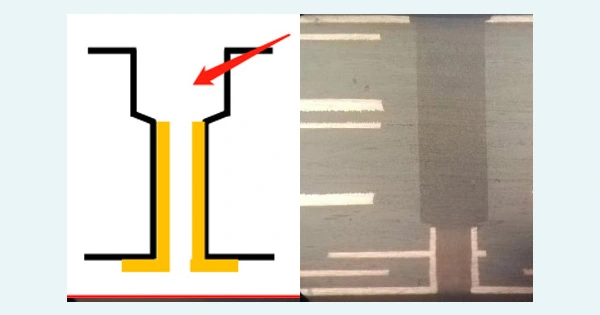
Backdrilling, also known as controlled-depth drilling, refers to the process of drilling from the backside of an already processed via to remove unwanted stubs. Backdrilling effectively reduces signal loss and enhances signal integrity, optimizing the overall performance of the PCB.
Why is Backdrilling Necessary?
In high-speed signal transmission, excess stubs (sections of the via that extend beyond the signal layers) can cause signal reflection, scattering, and delay, leading to signal distortion. Backdrilling eliminates these unnecessary stubs, reducing signal discontinuities and improving signal integrity, which minimizes noise interference and enhances circuit performance.
Typical Process Flow:
- Initial Via Processing: The standard drilling method is used to create through-holes that extend across the entire board thickness.
- Secondary Backdrilling: A larger diameter drill is used to re-drill from the backside and remove the copper stub to the specified depth.
- Precision Verification: Ensure that the backdrilling depth matches design specifications to avoid damage to the signal layers.
For example, in a 10-layer PCB design where signals need to be transmitted only from Layer 1 to Layer 3, the via processing leaves a stub below Layer 3. Backdrilling is used to remove the excess copper below Layer 3, reducing high-frequency interference.
Technical Characteristics and Design Requirements of Backdrilling
The key technical parameters for backdrilling include drill bit diameter, hole depth, stub length, and safety clearance. Below are the detailed explanations:
Drill Bit Diameter
The backdrill bit diameter is typically 0.15 to 0.2mm larger than the original via drill. For example, if the via drill diameter is 0.3mm, the backdrill bit should be 0.45 to 0.5mm.
Stub Length Control
Ideally, backdrilling should remove all stubs below the signal layers, but due to process tolerances, the remaining stub length usually ranges from 2 mils to 12 mils. A stub that is too short can cause open-circuit issues after soldering, so a balance must be struck between stub length and signal integrity.
Safety Clearance
The clearance between the backdrilled via edge and the surrounding traces should be at least 10 mils. In extreme cases, it can be reduced to 6 mils, but this increases production difficulty.
Process Tolerances
The tolerance of the finished board thickness can affect the accuracy of the backdrilling depth. For instance, if the designed board thickness is 4mm, the actual thickness could range from 3.6mm to 4.4mm. During production, backdrilling parameters must be adjusted based on the actual thickness to ensure safe distances from the signal layers.
PCB Issues Addressed by PCB Backdrilling
- Reduction of Signal Reflection and Interference: By removing the stubs, PCB backdrilling effectively reduces signal reflection and interference during transmission, enhancing signal clarity and stability.
- Improved Signal Integrity: PCB backdrilling minimizes the parasitic capacitance and inductance effects of vias, ensuring the full transmission of high-speed signals and preventing signal distortion.
- Reduction of Crosstalk: In high-frequency PCB designs, PCB backdrilling reduces crosstalk by shortening the via length, decreasing electrical coupling between adjacent traces, thus reducing interference and improving signal clarity.
- Minimized Noise Interference: By removing excess via segments, PCB backdrilling reduces unnecessary signal interference, thereby improving the transmission quality of the PCB.
Characteristics of PCB Backdrilling
- Suitable Materials: PCB backdrilling is commonly used in rigid PCBs, typically those with more than 8 layers and a board thickness greater than 2.5mm. When designing, it’s important to consider the board’s thickness and number of layers to ensure the feasibility and effectiveness of PCB backdrilling.
- Hole Diameter Requirements: The diameter of a PCB backdrilled hole is typically 0.2mm larger than the original via to effectively remove excess copper. The minimum diameter for the initial drill is generally ≥0.3mm.
- Depth Tolerance: PCB backdrilling requires precise control over hole depth to ensure that only excess via copper is removed, without damaging the necessary conductive layers. This requires drilling equipment with high-precision depth control, usually maintaining a depth tolerance within ±0.05mm.
- Design Considerations: During the PCB backdrilling design, it is crucial to ensure adequate spacing between the backdrilled holes, surrounding traces, and pads to avoid damaging other parts of the circuit.
PCB backdrilling technology improves signal integrity by accurately removing excess portions of vias, thereby reducing interference and signal distortion. However, the backdrilling process has higher design and manufacturing requirements, requiring precise depth control and careful design layout to ensure its effectiveness and reliability.