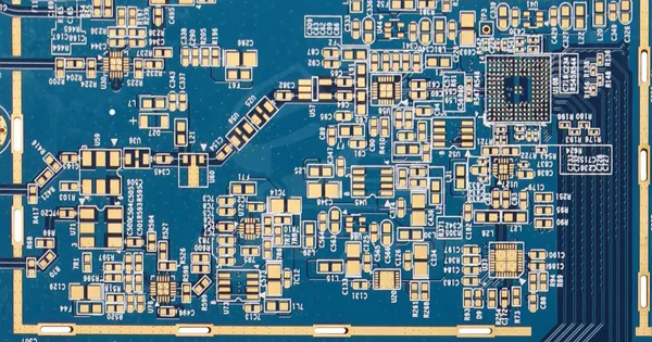
RF PCB design is a critical and complex aspect of electronics engineering, with its performance directly affecting the overall system's operation. The high-frequency characteristics of RF signals impose strict requirements on circuit layout. This article will delve into the key principles of
RF PCB circuit layout, helping designers optimize their designs in real-world projects to ensure the circuit performs as expected.
1. Signal Integrity: Optimizing High-Frequency Signal Paths
In RF PCB circuits, signal integrity (SI) is one of the core issues. Due to the high frequency of RF signals, even small design mistakes can lead to signal reflection, loss, or delay, ultimately affecting circuit performance.
1.1 Short Path Design
In RF PCB design, RF signal lines should be kept as short as possible. The reason is that longer paths increase transmission delay, and signal transmission over longer distances can easily lead to reflection and radiation loss. A short path not only reduces transmission time but also minimizes parasitic inductance and capacitance effects caused by line length, thereby improving signal integrity.
1.2 Impedance Matching
Impedance mismatch in RF PCB circuits can lead to signal reflection, affecting signal stability. Therefore, it is crucial to ensure that the trace's characteristic impedance matches the load impedance in the design. This is typically achieved by adjusting the trace width, the thickness of the dielectric material, and the trace spacing. Precise impedance matching can minimize reflection, making signal transmission more stable.
1.3 Trace Angles
When routing RF signals on an RF PCB, right-angle turns should be avoided, as right angles cause signal reflection and increase transmission loss. Instead, it is recommended to use 45-degree or smoother curves, which reduce signal reflection at corners and lower high-frequency loss.
2. Power Integrity: Designing Stable Power Supply
Power integrity (PI) is as important as signal integrity in RF PCB circuits. A stable power supply affects not only the overall circuit stability but also directly impacts RF signal quality.
2.1 Decoupling Capacitor Selection and Placement
In RF PCB circuits, decoupling capacitors should be placed near each critical power supply node. These capacitors filter out high-frequency noise from the power supply, providing a clean power signal to the circuit. When laying out, decoupling capacitors should be placed as close to the power pins as possible to minimize the impact of parasitic inductance.
2.2 Power and Ground Plane Design
To ensure power stability in RF PCB design, the power plane and ground plane should be closely coupled, reducing the parasitic inductance of the power supply and minimizing the impact of power noise on signals. A tightly coupled power and ground plane also form a low-impedance power path, ensuring the stability of power supply during high-speed operation.
2.3 Power Distribution Network (PDN) Design
The PDN is a critical part of RF PCB design, responsible for distributing power from the power module to every part of the circuit. In designing the PDN, consider power distribution, decoupling capacitor placement, and coupling between power and ground layers to ensure power signal integrity and stability.

3. Ground Plane Design: Optimizing Signal Return Paths
The ground plane in RF PCB circuits not only provides a current return path but also acts as a shield and isolates electromagnetic interference. A well-designed ground plane can effectively enhance the circuit's interference immunity.
3.1 Maintaining Ground Plane Integrity
Designers should avoid splitting the ground plane in RF PCB design, as it disrupts the signal return path, leading to increased return path length, which can cause signal reflection and interference. Therefore, maintaining the continuity and integrity of the ground plane is crucial, especially in areas with dense signals, where the ground plane should not be cut by vias or other traces.
3.2 Multi-Layer PCB Design
In high-density RF PCB circuits, using multi-layer PCBs can effectively separate signal layers from ground layers, reducing signal crosstalk and electromagnetic interference. In such designs, the power and ground planes are usually placed on adjacent layers to form good coupling, further reducing electromagnetic interference.
3.3 Coupling Between Signal Layer and Ground Layer
Tight coupling between signal and ground layers in RF PCB design can reduce the parasitic inductance and capacitance effects on signals, shorten the signal return path, and ensure signal stability. Therefore, in design, the distance between the signal layer and ground layer should be as close as possible to improve the reliability of signal transmission.
4. Electromagnetic Interference and Compatibility (EMI/EMC): Controlling the Electromagnetic Environment
RF PCB circuits, operating in high-frequency environments, are susceptible to electromagnetic interference (EMI) and can also be sources of electromagnetic noise. Good EMI/EMC design can reduce electromagnetic interference and ensure the circuit works properly.
4.1 Shielding Measures
In RF PCB circuits, shielding is one of the most effective ways to prevent electromagnetic interference. By using metal shields in the circuit or adding shielding layers in the PCB design, electromagnetic noise between the circuit and the external environment can be isolated. Additionally, shielding lines can be added in sensitive areas to further enhance anti-interference capability.
4.2 Application of Filters
In RF PCB design, filters are often needed at key nodes, especially at power inputs or sensitive signal paths. Filters can effectively suppress high-frequency noise, preventing it from spreading within the circuit, thus improving the circuit's electromagnetic compatibility.
4.3 Avoiding Noise Coupling
In RF PCB design, noisy signal lines should not run parallel or cross with sensitive signal lines. By rational layout design, reduce coupling between high-noise areas and sensitive areas, preventing electromagnetic interference from affecting signals.
5. Trace and Spacing Design: Optimizing Signal Transmission Paths
The design of signal traces in RF PCB circuits directly affects the quality of signal transmission. Reasonable trace design can reduce signal loss and interference, ensuring the stability of circuit performance.
5.1 Trace Width
The width of the trace in RF PCB design should be determined according to the frequency of the signal and the dielectric constant of the PCB material. Generally, the higher the signal frequency, the wider the trace should be to reduce transmission loss. The change in trace width should also consider impedance matching, avoiding discontinuous impedance caused by width changes, leading to signal reflection.
5.2 Trace Spacing
When designing high-frequency RF PCB circuits, the spacing between different signal lines should be large enough to reduce crosstalk between signals. Especially in high-speed signal transmission, the coupling effect between signal lines can degrade signal quality, so the spacing should be increased as much as possible, or shielding traces should be used to reduce crosstalk.
5.3 Differential Signal Traces
For some high-frequency RF PCB signals, such as high-speed serial data lines, differential signal transmission can be used. Differential signals have strong resistance to external interference and can also reduce the radiation of signal lines to the surrounding environment. In RF PCB design, the length of differential signal traces should be consistent to avoid signal transmission delay difference.
6. Common Layout Errors and Avoidance Methods
In practical RF PCB design, some common layout errors can lead to reduced circuit performance. Below are some common issues and how to avoid them:
6.1 Ignoring Ground Plane Integrity
Some designers do not pay attention to the integrity of the ground plane during layout, leading to signal path interruptions. Ensure the continuity of the ground plane and minimize cutting. An incomplete ground plane can lead to increased signal return paths, causing unnecessary electromagnetic interference.
6.2 Not Considering Signal Return Path
If the signal return path in RF PCB design is not reasonably designed, it may lead to unnecessary electromagnetic interference. Carefully plan the return path to ensure it is as short and direct as possible. Incorrectly planned return paths increase parasitic inductance, affecting signal stability.
6.3 Excessive Use of Vias
In RF PCB design, the use of vias should be minimized. Each via increases the parasitic inductance and capacitance effects of the signal, affecting the quality of signal transmission. Especially on high-frequency signal paths, too many vias can significantly degrade signal quality.
The layout design of RF PCB circuits is a complex and highly cautious process. By following the above RF PCB layout principles, designers can effectively reduce electromagnetic interference, ensure signal transmission integrity, and power stability, thereby improving the performance of the entire RF PCB circuit. In practical projects, designers should continuously optimize the layout according to specific application scenarios to achieve the best RF PCB design results.Partnering with
SprintPCB ensures that these design principles are expertly applied, providing you with high-quality RF PCB solutions that meet the stringent demands of modern electronics.

