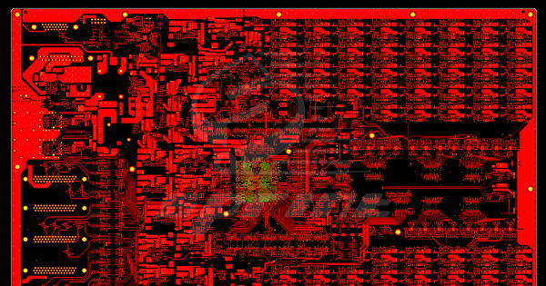
Signal integrity is one of the most critical aspects of PCB design, especially as the speeds of digital signals continue to rise in modern electronic devices. A failure to properly manage signal integrity can lead to data corruption, signal distortion, and malfunctioning circuits, all of which can severely affect the performance and reliability of electronic systems. This article explores the factors that influence signal integrity and provides actionable design tips to optimize signal quality in PCB design.
Key Factors Affecting Signal Integrity
Several factors can negatively impact signal integrity in a PCB design. These include noise, crosstalk, reflection, and electromagnetic interference (EMI). Each of these issues can lead to the degradation of the transmitted signal, causing errors, delays, or complete failure of communication between different components of the system.
Noise:
Noise is unwanted electrical interference that can disrupt the desired signal. It can originate from various sources, such as power supplies, nearby circuits, or external environmental factors. Noise can cause signal degradation by introducing spurious signals or by disturbing the original waveform of the transmitted signal.
Crosstalk:
Crosstalk occurs when signals from one trace or wire interfere with adjacent traces. It happens when the electrical fields of nearby signal lines influence each other, leading to unintended signal coupling. Crosstalk can result in false triggering or noise in neighboring signal paths, thereby compromising data integrity.
Reflection:
Reflection is the phenomenon that occurs when a signal encounters an impedance mismatch along its path. When the impedance of the signal trace does not match the impedance of the PCB material or the connected components, some of the signal is reflected back toward the source. This can cause signal distortion, phase shifts, or even complete data loss if the reflected signal interferes with the incoming signal.
Electromagnetic Interference (EMI):
EMI is the disruption caused by external electromagnetic fields. These fields can induce currents in the PCB traces, causing noise and signal distortion. High-speed circuits are particularly susceptible to EMI because their rapid switching can generate high-frequency signals that radiate outward and interfere with nearby electronic devices.

Design Considerations for Optimizing Signal Integrity
To optimize signal integrity in PCB design, designers must carefully consider factors such as
trace routing, material selection, grounding techniques, and
impedance control. Below are some of the most effective strategies for improving signal quality:
Differential Pair Routing:
Differential signaling is one of the most effective ways to mitigate noise and improve signal integrity. In this method, two complementary signals are sent along paired traces. The advantage of differential pairs is that the two signals cancel out common-mode noise. When routing differential pairs, it is essential to keep the traces close together to ensure that they experience the same impedance and are less susceptible to noise and interference.
Use of Ground Planes:
A solid ground plane beneath the signal traces is essential for minimizing noise and reducing signal distortion. The ground plane provides a low-resistance path for current return, which helps maintain signal integrity. It also shields sensitive signals from external EMI and reduces the potential for crosstalk. A continuous ground plane provides a stable reference voltage for the circuit, improving the overall performance of high-speed signals.
Impedance Matching:
Impedance mismatches are a leading cause of signal reflection. By ensuring that the impedance of the signal traces matches the impedance of the components and connectors they are connected to, signal reflections can be minimized. This can be achieved through careful trace width selection, controlled impedance routing, and selecting appropriate PCB materials with known and consistent dielectric properties.
Minimizing Trace Lengths:
Longer signal traces are more susceptible to noise and signal degradation. By keeping trace lengths as short as possible, the signal path is optimized, reducing the likelihood of reflections and interference. Additionally, minimizing trace lengths helps reduce the effects of parasitic inductance and capacitance, which can affect the timing and integrity of high-speed signals.
Signal Termination:
Signal termination is another technique used to prevent reflections in high-speed PCB designs. Proper termination ensures that signals are properly absorbed at the end of the transmission line rather than reflecting back toward the source. Common methods of signal termination include series, parallel, and resistive termination, depending on the specific requirements of the signal and the PCB layout.
Decoupling Capacitors:
Decoupling capacitors are essential for providing a stable power supply and reducing voltage fluctuations that can interfere with signal integrity. These capacitors help filter out high-frequency noise from the power rails and ensure that the signal voltage remains constant, reducing the likelihood of signal degradation due to power-related issues.
PCB Material Selection:
The material used for the PCB can have a significant impact on signal integrity. For high-speed circuits, it is essential to select materials with low signal loss and consistent dielectric properties, such as Rogers or Teflon. These materials help ensure that signals maintain their integrity over long distances and reduce the effects of impedance mismatch.
Shielding:
In certain high-speed PCB designs, shielding may be necessary to protect sensitive signals from external EMI. Shielding can be achieved through the use of conductive enclosures or copper traces that surround the sensitive signal traces. This method provides a barrier that prevents EMI from affecting the signal path and helps maintain signal integrity in noisy environments.
Optimizing signal integrity in PCB design is a critical aspect of ensuring the reliable performance of high-speed electronic systems. By addressing issues such as noise, crosstalk, reflection, and EMI, and implementing strategies such as differential pair routing, grounding techniques, and impedance matching, designers can significantly improve the quality and reliability of signals. With careful attention to detail, proper materials, and sound design practices, signal integrity can be maintained even in the most complex and demanding PCB designs.
As the demand for faster, more efficient electronic systems continues to rise, understanding how to optimize signal integrity will remain a key factor in successful PCB design. SprintPCB, as a leading manufacturer of high-quality PCBs, provides customers with the expertise and advanced design capabilities to create reliable, high-performance PCBs for a wide range of applications.

