Impedance control is a critical aspect in the design and manufacturing of high-speed PCBs, playing a pivotal role in maintaining signal integrity and ensuring reliable performance in advanced electronic systems. As the demand for faster, more efficient electronic devices continues to grow, especially in industries like telecommunications, automotive, and consumer electronics, understanding and applying proper impedance control techniques has become indispensable for designers and manufacturers.
What is Impedance Control?
Impedance control refers to the process of managing the electrical impedance of signal traces in a PCB to ensure that the impedance remains consistent throughout the circuit. Impedance is essentially the resistance to alternating current (AC) and is affected by the capacitance and inductance of the traces on the PCB. In high-speed circuits, even small variations in impedance can lead to signal reflection, distortion, and loss of data integrity. Therefore, achieving precise impedance matching is essential for high-performance PCBs, particularly when dealing with high-frequency signals.
Impedance is typically defined as the opposition that a circuit presents to the flow of an alternating current (AC) and is measured in ohms. In a PCB, impedance control is necessary to ensure that the signal travels along the PCB without significant reflection or attenuation, which could cause errors or data corruption in high-speed digital communication.
Factors Affecting Impedance Control
Several factors affect impedance control in PCBs. These include trace width, trace length, the thickness of the PCB substrate, the dielectric constant of the materials used, and the distance between signal traces and ground planes. Any of these factors, if not carefully controlled, can result in impedance mismatches that degrade signal quality.
1.Trace Width and Thickness:
The width and thickness of the trace determine its resistance. The narrower the trace, the higher the impedance. For high-speed signals, traces must be designed with a specific width to achieve the desired impedance level, typically 50 ohms for single-ended signals and 100 ohms for differential signals.
2.PCB Material and Dielectric Constant:
The material used for the PCB substrate, often FR4, BT, or polyimide, significantly impacts the dielectric constant (Dk) of the board. The dielectric constant defines how the material affects the velocity of the signal traveling through the PCB. Materials with a higher Dk value slow down signal propagation, while those with a lower Dk value speed up the signal. It is crucial to select materials with a known and stable dielectric constant to ensure consistent impedance.
3.Layer Stack-up Design:
The arrangement of layers in a PCB stack-up directly influences impedance control. For example, signal traces should ideally be placed between the ground and power planes, where the return path is well defined. By using controlled impedance traces, designers can ensure that the signals are transmitted with minimal distortion. Layer stack-up plays a significant role in controlling the differential impedance, particularly in multilayer PCBs.
4.Signal Trace Length:
Longer traces are more likely to experience impedance mismatches due to changes in signal path length. In high-speed PCBs, short and direct signal paths are preferred to minimize impedance variations and signal degradation. Signal integrity can be compromised if traces are too long, leading to higher levels of reflection and loss.
The Role of Impedance Control in High-Speed Signal Transmission
The importance of impedance control becomes especially evident in high-speed PCB designs. With the increasing speed of digital signals, high-frequency circuits are more susceptible to impedance mismatches. These mismatches can cause a variety of problems, including signal reflection, increased electromagnetic interference (EMI), and crosstalk between adjacent traces.
In high-speed systems, even a small reflection can result in data errors, which can cause significant performance issues. Impedance mismatch typically occurs when there is a difference between the impedance of the signal trace and the characteristic impedance of the transmission line, which is influenced by the PCB material, the trace width, and the distance between the trace and the ground plane. When the impedance is not matched, part of the signal is reflected back toward the source, causing signal degradation and loss of data integrity.
How to Achieve Impedance Control in High-Speed PCBs
Achieving precise impedance control in high-speed PCBs requires careful design and manufacturing practices. The following strategies are commonly used:
1.Stack-up Design:
Proper layer stack-up is crucial for controlling impedance. By strategically placing signal layers between power and ground planes, designers can create a controlled environment that minimizes signal interference and maintains impedance consistency.
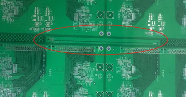
2.Trace Width and Spacing Control:
The width of the traces must be calculated to meet the required impedance. Manufacturers often use specialized software tools to simulate and optimize the trace widths for controlled impedance. Additionally, the spacing between traces, especially differential pairs, must be maintained to ensure proper impedance matching.
3.Use of Differential Pairs:
For high-speed signals, differential pairs are commonly used, where two traces carry complementary signals. By carefully managing the distance between these two traces, impedance can be controlled, and the signal integrity is preserved.
4.Material Selection:
Choosing the right PCB material is critical for maintaining a stable impedance. High-quality materials with consistent dielectric properties are essential for achieving precise impedance control. Materials such as Rogers, which offer lower signal loss and stable dielectric constants, are often used in high-speed designs.
5.Simulation and Testing:
Advanced simulation tools can be used during the design phase to model the impedance of traces and predict how they will behave under different conditions. This allows designers to make adjustments before manufacturing. After production, impedance testing using specialized equipment can verify that the PCB meets the required specifications.
Impedance control is a fundamental aspect of high-speed PCB design. By ensuring that the impedance of the signal traces remains consistent, designers can prevent signal degradation, reduce EMI, and ensure the overall performance of the PCB. Through careful attention to factors like trace width, material selection, and stack-up design, it is possible to create high-speed PCBs that deliver reliable, high-performance results.
As technology continues to advance, the need for high-speed, high-precision PCBs will only grow. By mastering impedance control techniques, manufacturers like SprintPCB can provide high-quality PCBs that meet the demands of modern electronic systems, ensuring their customers' success in a competitive marketplace.