In the era of modern technology, the development of electronic devices and systems has become increasingly rapid. One key component among them is the PCB, which serves as the foundation for connecting and supporting various electronic components in electronic devices. The quality and efficiency of its design are crucial for the overall performance of the system.
With the continuous advancement of technology, the emergence of advanced PCB design software has brought tremendous opportunities and challenges for PCB designers. These advanced software tools not only provide more powerful and intelligent design capabilities but also help designers improve work efficiency, accuracy, and creativity. There are multiple benefits to using advanced PCB design software. Firstly, these softwares provide intuitive and user-friendly interfaces, allowing designers to quickly grasp and start using them. Secondly, the software offers a wide range of design options, enabling designers to flexibly implement their design ideas and optimize and adjust them throughout the design process. Additionally, advanced PCB design software also features powerful simulation and validation capabilities, helping designers identify and resolve issues early in the design phase, thereby reducing errors and improving the design. In this article, we will delve into how to fully harness the potential of advanced PCB design software. We will introduce the features and characteristics of these software tools, as well as how they enhance design efficiency and accuracy. We will also discuss how these tools expand design possibilities, enabling designers to achieve better results in areas such as high-density layouts, high-speed signal transmission, and multilayer designs. Additionally, we will emphasize the importance of these software tools in team collaboration and version control, and we provide some suggestions and practical experiences to help readers choose and implement PCB design software that suits their needs.
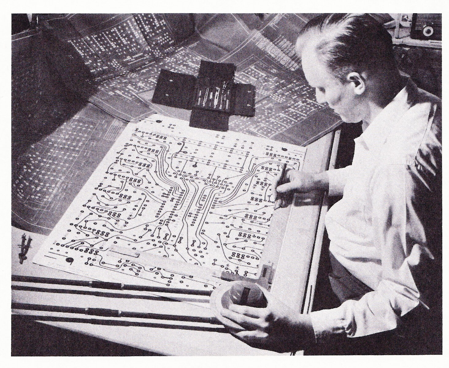
The PCB design has undergone significant evolution over the past few decades. From manual drawing in the beginning to advanced PCB design software today, this process has brought about notable improvements and increased efficiency. In the past, PCB design was done through manual drawing. Designers used pencils and rulers to draw circuit connections and component layouts on special design drafting paper. This manual drawing method was time-consuming and prone to errors. Any changes or fixes required redrawing the entire design, which limited the complexity and innovation of the design.
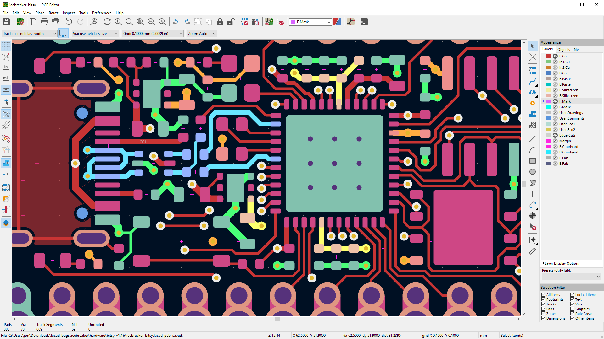
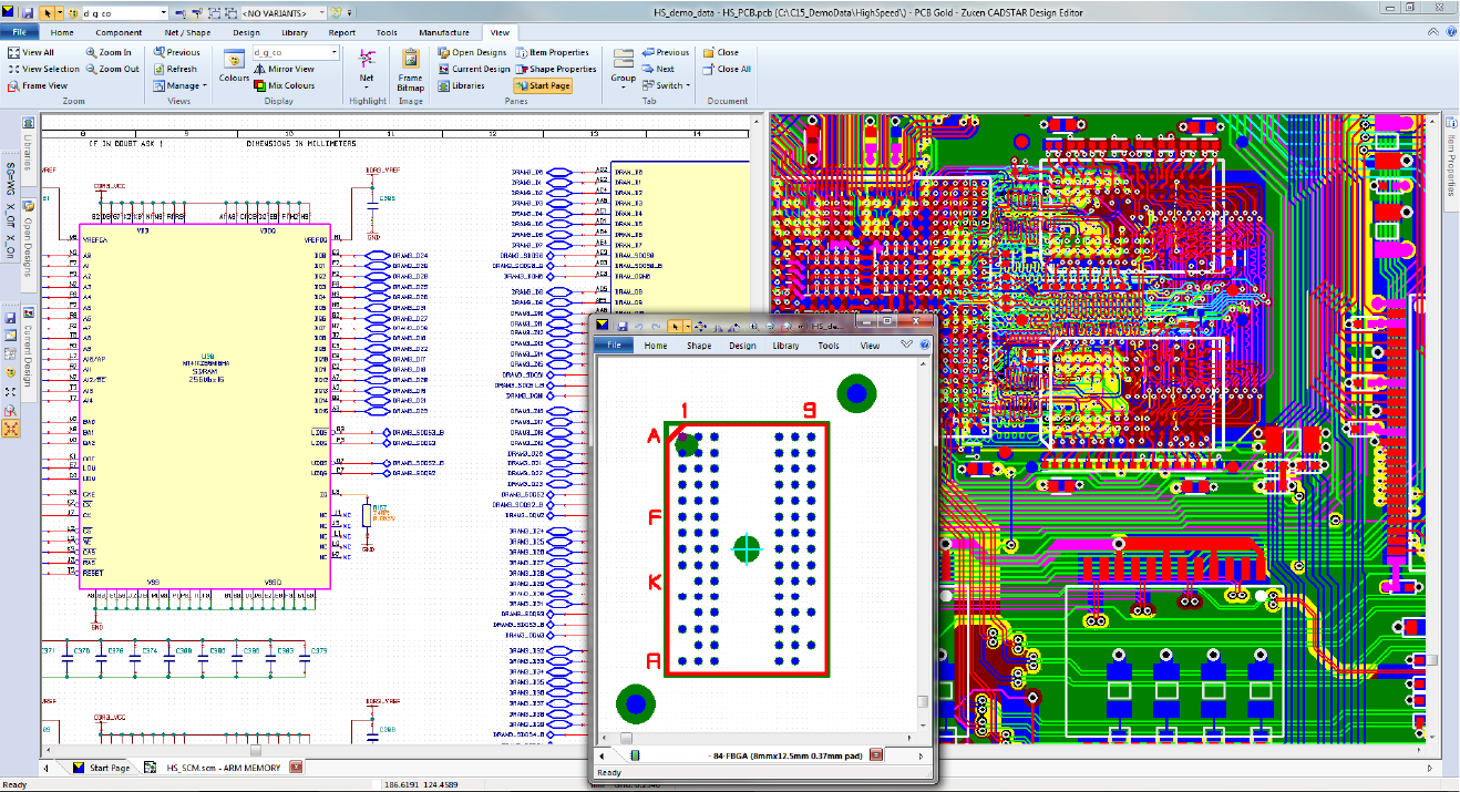
With the development of computer technology, the earliest PCB design software emerged. These software programs utilized simple 2D graphical interfaces, allowing designers to draw circuits and arrange components on computer screens. However, the functionality and performance of these software programs were limited, often only capable of handling basic circuit designs. Over time, advanced PCB design software has gradually emerged. These software programs introduce more powerful features and innovative design tools, enabling designers to handle more complex and high-density circuit designs. Advanced PCB design software utilizes a three-dimensional graphical interface, providing a more intuitive and visual design environment. Designers can freely rotate, zoom, and view the design, allowing for a better understanding of the circuit's structure and connections. Advanced PCB design software has also introduced many automation features, such as routing, signal integrity analysis, and component library management. These features enhance design efficiency and accuracy. Designers can use the automated routing tool to quickly complete circuit routing, reducing the occurrence of human errors. The signal integrity analysis tool can help designers predict and resolve issues such as signal interference, delay, and loss. The component library management tool enables designers to easily manage and reuse standard components, saving time and resources. In addition to basic functionalities, advanced PCB design software also offers numerous advanced features. For instance, the Design Rule Check (DRC) function can automatically detect and correct errors that violate circuit rules during the design process. Simulation and analysis tools can assist designers in evaluating circuit performance and optimizing designs. These advanced features enable designers to verify and optimize circuits with greater precision, ensuring the reliability and stability of the design. In addition, modern PCB design software also supports collaboration and version control among multiple individuals. Design teams can work simultaneously on the same design file, allowing real-time communication and resource sharing. The version control feature tracks the history of the design and enables team members to revert to previous design versions. This capability of collaboration and version control helps improve team efficiency and collaboration. In general, PCB design has undergone a significant evolution from manual drawing to advanced PCB design software. Advanced PCB design software offers more powerful, flexible, and efficient design tools, enhancing designers' capabilities and creativity. The development of these tools has made it possible to achieve more complex and innovative circuit designs, providing strong support for the development and advancement of electronic products.
Circuit Simulation and Analysis Function: Advanced PCB design software typically comes equipped with powerful circuit simulation and analysis tools. These tools allow designers to perform circuit simulations during the design phase to evaluate the performance, stability, and signal integrity of the circuit. Through simulation and analysis capabilities, designers can detect and address potential issues at an earlier stage, thereby enhancing design quality and reliability.
Layout and Routing Tools: Advanced PCB design software provides advanced layout and routing tools to help designers efficiently place and connect components on a PCB board. These tools can automatically optimize the layout, taking into consideration factors such as signal integrity, power noise, thermal management, and EMC. They can also provide real-time feedback and guidance, helping designers maximize performance and efficiency while meeting requirements.
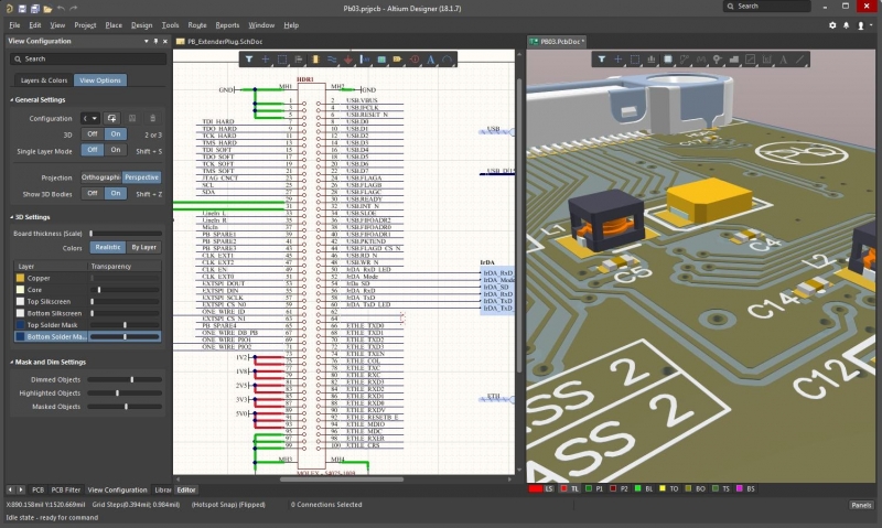
3D Design and Visualization: Advanced PCB design software often supports 3D design and visualization capabilities. This enables designers to view and inspect PCB boards in a three-dimensional format during the design process, gaining a better understanding of the interactions between components, physical constraints, and spatial requirements. Through 3D visualization, designers can better predict and address potential conflicts or errors and optimize designs to improve performance and manufacturing efficiency.
Automation and Optimization Features: Advanced PCB design software offers powerful automation and optimization features. These capabilities can automatically perform common design tasks such as routing, net planning, pin swapping, and package selection. Through automation and optimization, designers can save a significant amount of time and effort while enhancing the quality and consistency of their designs.
Material Management and Collaborative Design: Advanced PCB design software often includes integrated material management capabilities that help designers effectively manage component inventory, supply chain, and manufacturing requirements. Additionally, these software tools provide collaborative design features, allowing multiple designers to collaborate simultaneously and track and manage version control and change history of the design.
Communication and integration capability: Advanced PCB design software typically possesses excellent communication and integration capabilities with other tools and systems. For instance, they can integrate with electronic CAD (Computer-Aided Design) software, analog simulation tools, prototype manufacturing equipment, and PLM (Product Lifecycle Management) systems, enabling seamless flow and exchange of design data.
Error Detection and Verification: Advanced PCB design software comes with powerful error detection and verification capabilities, allowing real-time detection of potential issues during the design process. For example, the software can automatically check for wiring errors, component dimension mismatches, signal integrity problems, and more in the circuit layout. By identifying and rectifying these issues early on, designers can avoid costly errors and rework during the later manufacturing stages.
Automated and Intelligent Layout: Advanced PCB design software offers automated layout and routing tools that reduce the need for manual operations. By utilizing intelligent layout algorithms, the software can automatically optimize component placement and wiring paths to minimize signal interference, electromagnetic interference, and circuit noise. This automated layout feature not only saves designers' time but also enhances design accuracy and performance.
Design Rule Check (DRC): Advanced PCB design software includes comprehensive design rule check capabilities to ensure compliance with industry standards and specifications. Design rules can include requirements for component spacing, signal integrity, electrical specifications, pad sizes, and more. By automating the design rule check process, the software can assist designers in timely identifying and resolving potential issues, ensuring accuracy and reliability in the design.
Simulation and Analysis Tools: Advanced PCB design software often integrates powerful simulation and analysis tools, such as electromagnetic simulation, thermal analysis, and timing analysis. These tools assist design engineers in conducting virtual testing and optimization during the design stage to predict and address issues in the circuit. By utilizing simulation and analysis tools, design engineers can evaluate the performance, stability, and reliability of the circuit in advance, thus avoiding costly experimentation and manufacturing expenses.
Real-time collaboration and version control: Advanced PCB design software offers real-time collaboration and version control features, enabling convenient collaboration and communication among team members. Designers can simultaneously edit and annotate the same design file, while viewing the changes made by others in real-time. Additionally, the software can track and manage different versions of design files to prevent data loss or confusion.
By leveraging these features provided by advanced PCB design software, designers can greatly enhance design efficiency and accuracy. Such tools and functionalities enable designers to complete complex layout and routing tasks more quickly, reducing the risks of errors and rework, and improving the quality and reliability of the design.
High-density layout: Advanced PCB design software offers greater design flexibility, particularly in high-density layouts. By utilizing advanced layout tools and automated routing features, designers can effectively utilize space and place components within compact areas, enabling smaller, lighter, and more efficient electronic product designs.
High-Speed Signal Transmission: In modern electronic devices, high-speed signal transmission has become increasingly common. Advanced PCB design software provides dedicated tools and features to meet the demands of high-speed signal transmission. For example, designers can use signal integrity analysis tools to predict and address signal integrity issues, ensuring reliable transmission of high-speed signals on the PCB while reducing signal distortion and interference.
Multilayer Design: Advanced PCB design software supports multilayer design, enabling more complex circuits and functionalities to be realized within a smaller space. By distributing the circuits across different layers, designers can reduce electromagnetic interference, cross-coupling, and noise issues. Additionally, multilayer design can provide better isolation performance, enhancing the reliability and performance of the product.
3D Modeling and Simulation: Advanced PCB design software not only provides 2D design views but also supports 3D modeling and simulation capabilities. This allows designers to simulate and evaluate circuit performance, predict potential thermal issues, mechanical conflicts, electromagnetic interference, and more accurately. By conducting 3D simulations during the design phase, it is possible to reduce time and costs associated with prototype manufacturing and testing.
Specialized Technical Support: Advanced PCB design software such as Altium Designer, Cadence Allegro, Mentor Graphics PADS, and Eagle also provide support for special technologies such as embedded components, flexible circuit boards, and RF design. These technologies often have unique design requirements and constraints, and advanced PCB design software can provide tools and rules to simplify these complexities, helping designers better address the challenges. By utilizing these advanced PCB design software features, designers can gain more flexibility and creativity in the process of electronic product development. These software tools provide more powerful tools and analysis capabilities to help designers optimize designs, enhance performance, and maximize the potential of circuit boards.
Team Collaboration Features: Modern PCB design software provides various collaboration features that allow design teams to work together on the same project simultaneously. These features can include real-time collaboration, shared design files, commenting and annotations, task assignment and tracking, and more. Through these features, team members can collaborate more effectively, accelerate the design cycle, address issues, and communicate in a timely manner.
Version Control: Version control is key to maintaining the integrity and traceability of design files. Advanced PCB design software often integrates version control systems that track and manage the history of design files. This allows team members to easily revert to previous versions, compare differences, merge changes, and ensure that all modifications are properly documented and managed. Version control also helps resolve design conflicts and prevent unnecessary errors.
Collaborative Design: Collaborative design is a method of collaboration that integrates the work of multiple designers into a cohesive design. Advanced PCB design software offers collaborative design capabilities, allowing multiple designers to work simultaneously in the same design environment. This enables timely integration and coordination of modifications made by different designers, reducing errors, and enhancing design efficiency.
Permission Management: Permission management is necessary for team collaboration to control access to design files, ensuring that only authorized team members can make modifications and access them. Advanced PCB design software offers flexible permission management features that allow different levels of access based on team roles and responsibilities. In this way, administrators can control who can edit, view, or have read-only access to design files, ensuring the security and confidentiality of the designs. By fully leveraging the team collaboration and version control features, PCB design teams can achieve more efficient collaboration, reduce design errors and conflicts, and improve overall design quality. Team members can work simultaneously and share information and feedback in real time, thereby accelerating project progress and reducing risks.
Before choosing PCB design software that suits your needs, there are several key factors to consider. These factors will ensure that you can maximize the potential of advanced software and meet your project requirements. Firstly, you should clarify your functional requirements. Different software offers various functionalities and tools, so you need to determine the features your project requires. For instance, you may need a powerful circuit simulation tool, advanced layout and routing capabilities, support for embedded system design, and so on. Make a list of your functional requirements and ensure that the software can meet these needs. The user interface and ease of use of software are crucial for work efficiency and the learning curve. Choosing software with an intuitive interface and user-friendly design can help you get started quickly and improve productivity. Some software also provides interactive tutorials and training resources to help users better understand the features and usage techniques of the software. Considering the compatibility and integration of software is also crucial. You may need to integrate with other tools or systems such as CAD software, simulation tools, or material management systems. Ensure that the chosen software can seamlessly integrate with your existing tools and processes to better support your project. Choosing a software supplier that provides good technical support and training is also a wise choice. During the implementation and use of the software, you may encounter issues or require assistance. Ensure that the supplier is capable of providing timely technical support and offering training resources so that you and your team can fully leverage the software's functionalities. Finally, considering the cost and licensing models of the software is also important. Different software vendors may have different licensing models, such as subscription-based, perpetual licensing, or on-demand licensing. Evaluate the cost of the software and match it with your budget and project requirements. When implementing PCB design software, here are some best practices and recommendations: Establish a project team responsible for software selection, implementation, and training. Conduct software evaluation and demonstrations. Collaborate with vendors to understand the software's features, performance, and suitability. Develop a training plan to ensure team members acquire the necessary skills and best practices for using the software. Define an implementation plan and ensure sufficient time is allocated for software installation, configuration, and integration. Conduct trial runs and testing to ensure the software meets the requirements of actual projects. Monitor the performance and effectiveness of the software and make necessary optimizations and adjustments. By carefully considering software selection and implementation processes, you can ensure the choice of suitable PCB design software and successfully apply it to your projects.
In the communication industry, advanced PCB design software plays a crucial role in the manufacturing of communication equipment. For instance, a company may utilize such software to design and optimize circuit boards for wireless base stations, ensuring efficient and stable signal transmission. By leveraging the advanced simulation and analysis tools provided by the software, design teams can predict and address potential interference issues, thereby enhancing the performance of communication devices. Automotive Electronics: In modern cars, there is an increasing number of electronic components, which imposes higher demands on PCB (Printed Circuit Board) design. Advanced PCB design software can assist automobile manufacturers in achieving more compact and high-density designs in onboard electronic systems.

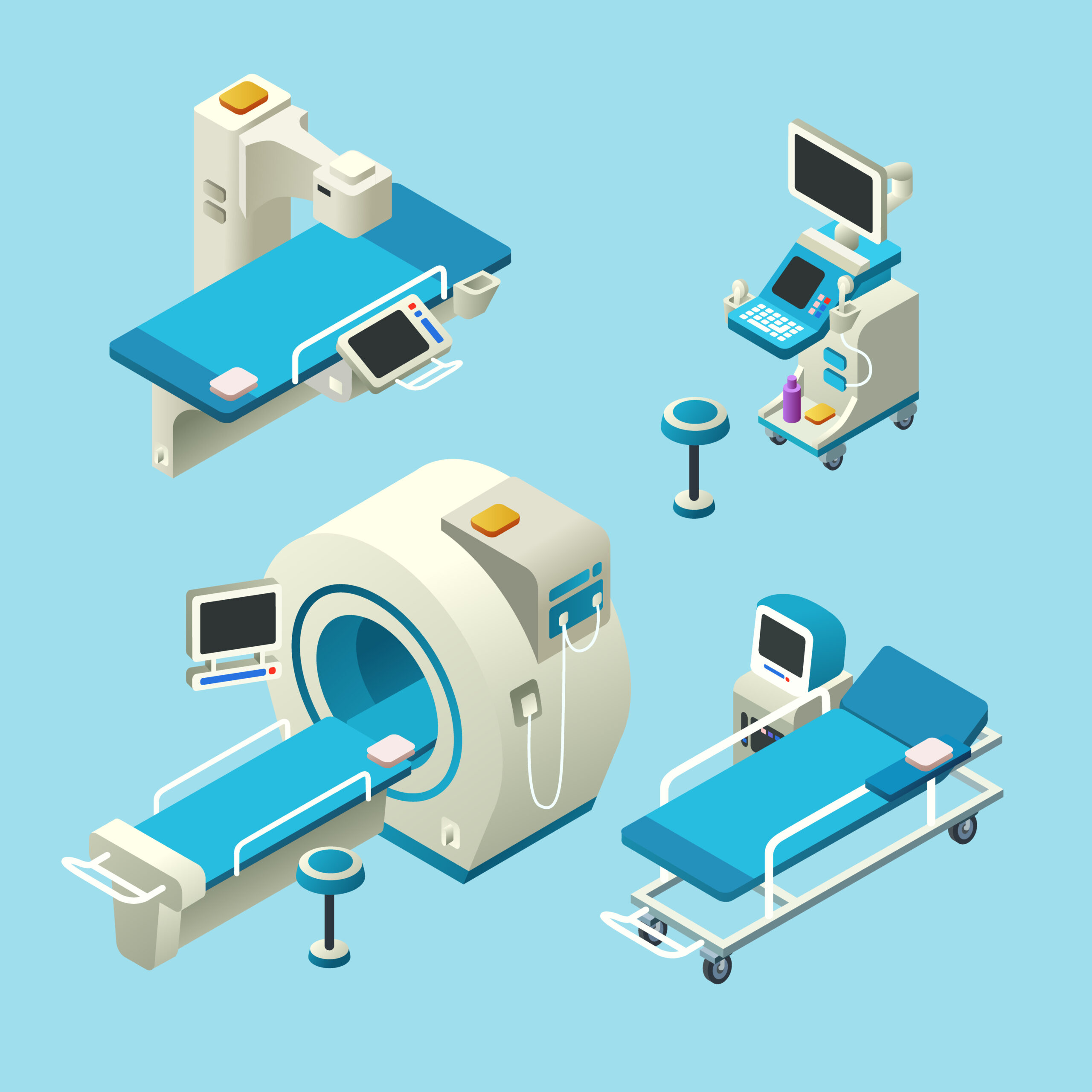
With the 3D modeling and simulation capabilities provided by the software, design teams can optimize the layout of circuit boards, ensure proper connections between components, and reduce the risk of electromagnetic interference. Medical Equipment: The design of medical equipment requires highly reliable and precise circuit boards. Advanced PCB design software enables medical equipment manufacturers to achieve higher design accuracy and quality control. For example, in the design process of a pacemaker, software can assist the design team in electrical simulation and analysis, ensuring the proper functioning of the device and compliance with medical standards and safety requirements.
Industrial Automation: In the field of industrial automation, PCB design software has a wide range of applications. For example, a manufacturer may use this software to design circuit boards for control systems, enabling the efficient operation of automated production lines. The software can assist the design team in conducting timing analysis and optimization, ensuring the coordination and accuracy of various control components, thereby enhancing production efficiency and quality.

Internet of Things (IoT): With the rapid development of the Internet of Things, advanced PCB design software plays a crucial role in the design of connected devices and sensors. By utilizing the routing and tracing tools provided by the software, design teams can achieve compact and low-power designs that meet the requirements of IoT devices. For instance, various sensors and controllers in smart homes and smart cities can be highly integrated and optimized through advanced PCB design software.

By using advanced PCB design software, we can achieve more efficient, accurate, and innovative circuit board designs. Modern PCB design software has many powerful features and capabilities that significantly improve design efficiency and provide designers with greater freedom. Finally, I hope this blog post can provide you with important information and insights about advanced PCB design software. If you want to learn more about PCB design software, I recommend you explore the relevant resources and links on the SprintPCB official website. Wishing you more success in the field of PCB design!

Customer support