As electronic devices become smaller, faster, and more powerful, the demand for more sophisticated internal components grows. While simple electronics can use single or double-sided boards, the complex products that define our modern world—like smartphones, high-end computers, and medical equipment—require a more advanced solution: the Multilayer PCB. As a premier manufacturer in the industry, SprintPCB specializes in the precision engineering required for these complex boards. This guide will explain what a Multilayer PCB is, its key advantages, and why choosing the right manufacturing partner is essential for your project's success.

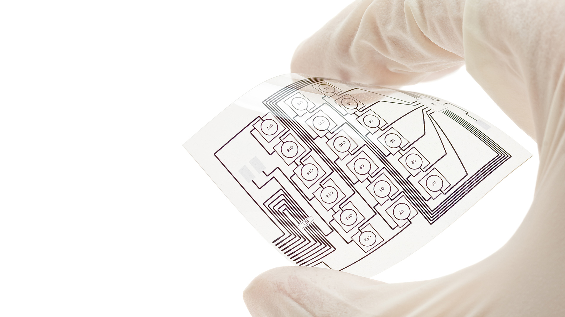
A Multilayer PCB is a printed circuit board composed of more than two conductive copper layers. Think of a simple double-sided PCB as a single-story building with a front and back yard. A Multilayer PCB, in contrast, is like a multi-story skyscraper. It sandwiches several double-sided PCBs together, separated by insulating layers, creating a single, compact board with numerous layers for routing electrical signals. These boards can range from a simple 4-layer construction to incredibly complex designs with 50 layers or more. This layered approach allows circuit designers to pack an enormous amount of electronic functionality into a very small space.
Why would a designer choose a more complex Multilayer PCB over a simpler board? The benefits are significant, especially for advanced electronics.
· Increased Density and Smaller Size: This is the primary advantage. By stacking layers vertically, designers can create highly dense and complex circuits in a much smaller footprint. This is crucial for miniaturization in devices like smartwatches, GPS trackers, and other portable electronics.
· Enhanced Electrical Performance: Multilayer PCBs allow for dedicated ground and power plane layers. These planes reduce electronic noise (EMI), minimize crosstalk between signals, and provide for controlled impedance, which is critical for maintaining signal integrity in high-speed circuits. The result is a more stable, reliable, and faster-performing product.
· Greater Design Flexibility: With more layers to work with, designers have more freedom in routing power and signal traces. This simplifies the design process for complex circuits that would be impossible to route on a single or double-sided board.
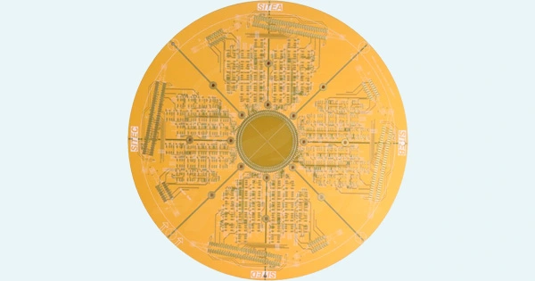
Creating a Multilayer PCB is a sophisticated manufacturing process that requires absolute precision. The board is built by laminating multiple "cores" and "prepreg" layers together under high temperature and pressure. A core is essentially a double-sided PCB, while prepreg is a fiberglass cloth pre-impregnated with resin that acts as the glue to bond the layers. During this process, it's critical to ensure perfect alignment between the layers.
One of the key technologies in Multilayer PCB fabrication is the creation of vias—the copper-plated holes that connect the different layers.
· Through-Hole Vias: These go through the entire board, from the top layer to the bottom layer.
· Blind Vias: These connect an outer layer to one or more inner layers but do not go all the way through the board.
· Buried Vias: These connect two or more inner layers and are completely invisible from the outside of the board.
The use of blind and buried vias frees up valuable surface space, allowing for even higher component density. The complexity of this lamination and drilling process is why working with an expert manufacturer is so important.
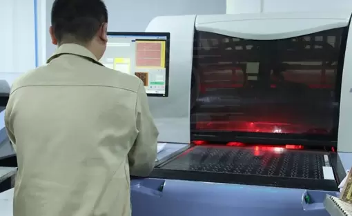
The quality of a Multilayer PCB directly impacts the performance, reliability, and lifespan of your final product. Flaws in layer alignment, lamination, or via drilling can lead to catastrophic failures. At SprintPCB, we have invested heavily in the state-of-the-art technology and process control needed to produce the highest quality Multilayer PCBs. Our engineering team works closely with clients to review their designs, ensuring they are optimized for manufacturability and performance. We have deep expertise in managing controlled impedance, fabricating complex via structures, and performing rigorous testing to guarantee that every board meets the most demanding specifications. When your project requires the complexity and performance of a Multilayer PCB, you need a partner you can trust. Contact SprintPCB to bring your advanced electronic designs to life.

Customer support