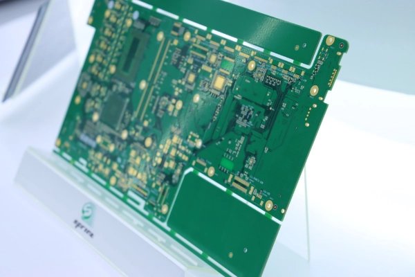
In the rapidly evolving world of electronics, the demand for smaller, faster, and more powerful devices is relentless. From the smartphones in our pockets to the complex systems guiding autonomous vehicles, the push for miniaturization and enhanced functionality is a constant driving force. At the heart of this revolution lies a critical component: the High-Density Interconnect (HDI) Printed Circuit Board (PCB). As a leading manufacturer in the PCB industry, SprintPCB is at the forefront of delivering high-quality HDI PCB solutions that empower innovation.

So, what sets an HDI PCB apart from a conventional circuit board? The name itself provides a clue. A High-Density Interconnect PCB is a type of printed circuit board that boasts a significantly higher wiring density per unit area. This is achieved through a combination of advanced manufacturing techniques that allow for finer lines and spaces, smaller vias (electrical connections between layers), and a higher connection pad density. Think of it as packing more electrical pathways and components into a much smaller and more efficient space.
The key technologies that define HDI PCBs include:
· Microvias: These are laser-drilled vias that are typically 150 microns or less in diameter. They are the cornerstone of HDI technology, enabling designers to place more connections in a smaller area. Microvias can be blind (connecting an outer layer to an inner layer) or buried (connecting two or more inner layers without reaching the outer layers), which frees up valuable surface space.
· Fine Lines and Spaces: Advanced imaging and etching processes allow for the creation of extremely narrow conductive traces and minimal spacing between them. This is crucial for routing the complex web of signals found in modern electronic devices.
· Sequential Lamination: HDI PCBs are often built up layer by layer. This sequential lamination process, where each new layer is added and then drilled for microvias, allows for the creation of highly complex, multi-layered boards that would be impossible to produce with traditional methods.
· Via-in-Pad: This technique involves placing vias directly on the surface mount pads of components. This further shortens the signal paths, improving electrical performance and freeing up even more space for routing on the board's surface.
At SprintPCB, we have mastered these intricate processes to produce HDI PCBs that meet the most stringent specifications. Our state-of-the-art facilities and experienced engineering team ensure that every board we produce offers exceptional reliability and performance.
The decision to use an HDI PCB is driven by a host of benefits that directly address the challenges of modern electronic design. For our clients, the advantages translate into superior products and a competitive edge.
The most obvious benefit of HDI PCB technology is the ability to create smaller and lighter products. By packing more functionality into a smaller board, designers can shrink the overall size of their devices. This is particularly critical in handheld electronics like smartphones and tablets, wearable technology, and medical implants where size and weight are paramount concerns.
Shorter signal paths mean better signal integrity. The microvias and fine lines in an HDI PCB reduce signal reflection, crosstalk, and electromagnetic interference (EMI). This results in faster signal transmission, lower power consumption, and improved overall performance, which is essential for high-frequency applications in telecommunications, computing, and aerospace.
The advanced manufacturing processes used for HDI PCBs result in a more robust and reliable product. The use of smaller vias and thinner dielectric materials can improve the board's resistance to thermal stress and mechanical shock. At SprintPCB, we adhere to the strictest quality control standards to ensure that our HDI PCBs can withstand the rigors of their intended applications.
While the initial cost of an HDI PCB might seem higher than a conventional board, it can often be more cost-effective in the long run for complex designs. By reducing the layer count and overall size of the board, HDI PCBs can lead to lower material costs and a more streamlined manufacturing process for the final product. The increased routing density can turn a complex 10-layer standard PCB into a more efficient 6-layer HDI PCB, saving both space and cost.
Creating an HDI PCB is a highly sophisticated process that demands precision at every stage. At SprintPCB, we have refined our manufacturing workflow to ensure the highest levels of quality and consistency. Here's a simplified overview of the key steps involved:
1. Core Lamination and Drilling: The process often begins with a standard core material, similar to a conventional PCB. This core may be drilled with traditional mechanical drills for through-hole vias if needed.
2. Sequential Build-Up: This is where the HDI magic happens. Thin layers of dielectric material and copper foil are laminated onto the core.
3. Laser Drilling: A high-precision laser is used to drill the microscopic microvias into the newly added layer. This process is incredibly fast and accurate, capable of creating thousands of vias in a matter of seconds.
4. Plating and Filling: The microvias are then plated with copper to create the electrical connection. They can also be filled with conductive or non-conductive epoxy to create a flat, planar surface for subsequent layers or component mounting.
5. Etching and Imaging: The circuit pattern for that layer is created through photolithography and etching, defining the fine lines and spaces.
6. Repeat: This build-up process of lamination, drilling, plating, and etching is repeated for each additional layer until the desired complexity and layer count are achieved.
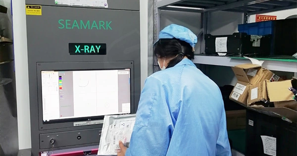
7. Final Finishing: The board undergoes final processing, including the application of a solder mask, surface finish (like ENIG or OSP), and electrical testing to ensure it meets all specifications.
This iterative, layer-by-layer approach gives designers unprecedented freedom but also requires close collaboration with the manufacturer. The team at SprintPCB works closely with clients from the design phase through to production to ensure optimal results and a seamless manufacturing experience.
The impact of HDI PCBs can be seen across a vast spectrum of industries. Wherever there is a need for high performance in a compact space, you will likely find HDI technology at work.
· Automotive: Modern vehicles are packed with electronics, from engine control units (ECUs) and infotainment systems to advanced driver-assistance systems (ADAS). HDI PCBs are essential for these applications due to their reliability and ability to withstand the harsh automotive environment.
· Aerospace and Defense: In aerospace applications, performance and reliability are non-negotiable. HDI PCBs are used in avionics, missile guidance systems, and communication equipment where space is at a premium and failure is not an option.
· Medical Devices: From diagnostic imaging equipment to life-saving implants like pacemakers and neurostimulators, HDI PCBs enable the creation of sophisticated medical devices that are both powerful and biocompatible.
· Telecommunications: The infrastructure that powers our connected world, including routers, switches, and base stations, relies on HDI PCBs to handle high-speed data transmission with minimal signal loss.
Choosing the right manufacturing partner is crucial for the success of any project involving HDI PCBs. At SprintPCB, we understand the complexities and challenges of this advanced technology. Our commitment to quality, innovation, and customer satisfaction sets us apart as a leader in the PCB industry.
When you partner with us through SprintPCB, you gain access to:
· Unmatched Expertise: Our engineers have years of experience in designing and manufacturing HDI PCBs for a wide range of applications. We provide expert guidance to help you optimize your design for manufacturability and performance.
· Cutting-Edge Technology: We continuously invest in the latest equipment and technologies, including advanced laser drilling systems and automated optical inspection (AOI), to ensure the highest levels of precision and quality.
· Commitment to Quality: We are certified to the highest industry standards, and our rigorous quality control processes ensure that every HDI PCB we produce is free from defects and meets your exact specifications.
· Customer-Centric Approach: We believe in building long-term partnerships with our clients. Our dedicated support team is always available to answer your questions and provide you with the support you need throughout the entire process.
The future of electronics is undeniably tied to the continued advancement of technologies like HDI PCBs. As devices become more integrated and intelligent, the need for smaller, faster, and more reliable circuit boards will only grow. SprintPCB is proud to be a part of this journey, providing the foundational components that enable our clients to turn their innovative ideas into reality. We invite you to contact us to learn more about our HDI PCB capabilities and how we can help you with your next project.

Customer support