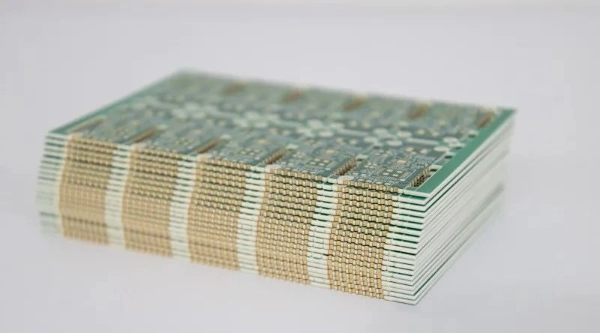
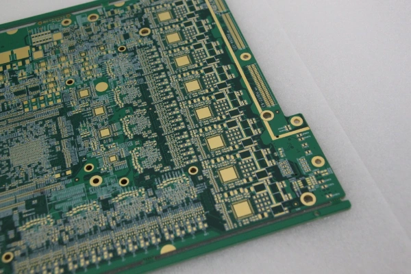
In printed circuit board (PCB) design, blind and buried vias are two crucial interconnection technologies that play a significant role in the manufacturing of high-density, high-performance electronic devices. This article will delve into the definitions and applications of blind and buried vias, as well as their creation processes. Additionally, we will introduce essential guidelines to consider when designing these special types of through-holes to ensure the reliability and performance optimization of the PCB. Let's explore the significance of blind and buried vias in modern electronic manufacturing and their design principles together.Blind and buried vias are two common types of plated through-hole structures in printed circuit board (PCB) design and manufacturing. They play crucial roles in connecting wires and signals across different layers. However, they have distinct design and manufacturing methods, catering to different application requirements.
Blind Vias:
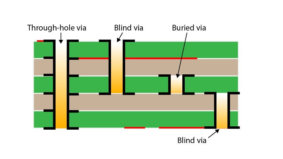
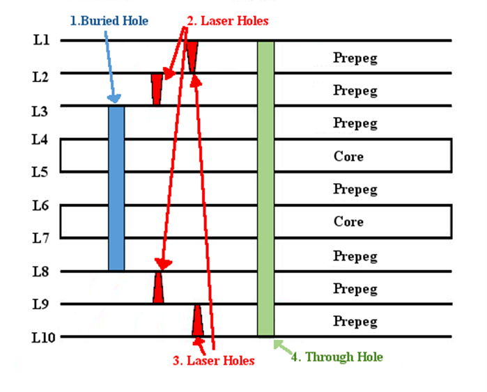
In PCB design, Blind Vias are a special type of plated through-hole (PTH) that connects only the outer layers to one or more inner layers without traversing the entire PCB. This design allows for necessary connections to be established within limited space while avoiding interference on the opposite side of the circuit board.
Definition and Purpose: Blind Vias are a type of PTH structure that connects the outer layers of a PCB to one or more inner layers but does not extend through the entire PCB. This means that Blind Vias are visible from one side of the board and "blind" or invisible from the other side.
Application Example: Let's consider a four-layer PCB where a connection is required between the first and second inner layers, while avoiding penetration through to the outermost layer of the PCB. In this scenario, Blind Vias can be used to achieve this connection without leaving unnecessary holes on the other side of the PCB.
Buried Vias:
Another common type of through-hole is Buried Vias, which connect one or more inner layers of a PCB but do not extend to any outer layers. Buried vias play a crucial role in complex multi-layer PCB layouts, especially in high-performance electronic devices where requirements for signal integrity and spatial optimization are extremely high.
Definition and Purpose: Buried vias are a type of through-hole structure that connects one or more inner layers of a PCB but does not extend to any outer layers, meaning they are completely hidden within the internal layers of the PCB.
Application Example: Consider a complex eight-layer PCB where multiple connections are needed between inner layers, without involving any outer layers. In this scenario, using buried vias is highly appropriate as they can achieve the required signal connections within the internal layers of the PCB while maintaining a clean appearance on the outer layers.
The drilling stage in the PCB manufacturing process is crucial for creating blind and buried vias. By controlling the depth of the drill holes, manufacturers can achieve selectively interconnected blind and buried vias, followed by plating processes to ensure the reliability of electrical connections.
Manufacturing process of blind vias:
Firstly, the normal drilling operation is performed on one side of the PCB to create vias from the outer layer to the inner layer.
Next, using controlled depth drilling technology, the drilling is limited to specific inner layers, without extending through to the other side of the PCB.
Finally, vias are plated to establish a conductive connection between the inner and outer layers.
Example: Let's consider a double-sided PCB where a connection needs to be established between the first and second layers, but without affecting the bottom second layer of the PCB. By controlling the depth of the blind vias, the drilling depth can be limited to only the space between the first and second layers, achieving the desired signal connection.
Manufacturing process of buried vias:
During the drilling stage of the manufacturing process, the depth of the vias is controlled to ensure that the drilling only remains within the inner layers of the PCB and does not extend to the outer layers.
Subsequently, these inner layer vias are plated to establish connections between the corresponding inner layers.
Example: Consider a complex multilayer PCB with four inner layers, requiring multiple signal connections between these layers. Through the manufacturing process of buried vias, these signal connections can be completely concealed within the internal layers of the PCB, without affecting the outer layers, thereby achieving higher routing density and improved signal integrity.
Overall, blind and buried vias provide PCB designers with more flexible options to meet the demands of high-density routing and complex signal routing. Their proper utilization contributes to improving the performance and reliability of PCBs.
Essential guidelines
When designing blind and buried vias, there are some essential guidelines that need to be followed to ensure the reliability, performance, and manufacturability of the PCB. The following is a detailed description of these guidelines along with relevant examples.
Aspect Ratio of Vias:
Definition: The aspect ratio of vias refer to the ratio between the depth and the diameter of the hole. This factor is particularly important in high-density PCBs, especially when using blind and buried vias.
Guidelines: To avoid manufacturing difficulties and improve reliability, it is generally essential to control the aspect ratio within a reasonable range. Higher aspect ratios can increase the challenges in drilling holes and plating, potentially leading to manufacturing issues such as uneven via walls or signal loss.
Example: Let's consider designing a high-density multi-layer PCB that requires the use of blind vias to connect outer and inner layers. To ensure a controlled aspect ratio, it might be necessary to optimize the board thickness and hole diameter to avoid excessively steep hole structures.
Annular Ring:
Definition: An annular ring is a copper pad surrounding a via, connecting the pad to a blind or buried via. It is crucial for providing a stable soldering connection.
Guideline: Ensure that the annular ring is sufficiently large to provide a reliable soldering area and a good connection. Too small annular rings may lead to weak solder joints and even connection issues during the manufacturing process.
Example: Consider a PCB application that requires high-temperature soldering. If the annular ring is too small, it may result in poor soldering, thereby affecting the reliability of the connection.
Trace and Via Spacing:
Definition: Trace refers to the conductive paths on a PCB, and the spacing between traces and blind/buried vias refers to the distance between the traces and the vias.
Guidelines: Sufficient spacing between traces and vias is essential to avoid signal interference and crosstalk. This is particularly critical in high-speed signal transmission designs to prevent signal attenuation and crosstalk.
Example: When designing a PCB for high-speed data transmission, insufficient spacing between traces and blind vias could lead to signal attenuation and data transmission errors.
Via Stubs:
Definition: Via stubs refer to the portions that extend from the end of a blind via/buried via, usually referring to the inner layers connected to the board.
Guideline: In high-frequency applications, it is advisable to minimize the length of via stubs to prevent impedance mismatches and signal reflections. Longer via stubs can lead to signal distortion and reduced transmission performance.
Example: When designing PCBs for wireless communication devices, it is essential to shorten the portions of blind vias connected to the inner layers to ensure high-quality signal transmission.
Interlayer Transition:
Definition: Interlayer transition refers to the process of signal trace switching from one layer to another, particularly when using blind vias.
Guidelines: The smoothness of interlayer transitions should be considered during the design process to avoid sudden changes in signal impedance. Transitions should be as gradual as possible to ensure signal integrity.
Example: When designing a multi-layer PCB for high-speed signal transmission, careful planning of signal trace paths is necessary to ensure signal stability during interlayer switching.
Thermal Considerations
Definition: Thermal considerations are necessary when using buried vias, as they may affect the heat flow within the PCB.
Guidelines: Careful consideration of thermal vias and copper distribution is essential during the design phase to ensure efficient conduction and dissipation of heat, thereby maintaining the operating temperature of electronic components within a safe range.
Example: When designing a PCB for a high-power power supply module, the positioning of buried vias must be taken into account to optimize thermal conduction and dissipation, ensuring that the component temperature remains within an acceptable range.
Following these guidelines can help ensure the smooth design and manufacturing of blind and buried vias, thereby guaranteeing the performance, reliability, and manufacturability of the PCB.
In summary, blind and buried vias, as advanced PCB connection technologies, provide powerful solutions for the manufacturing of high-density and high-performance electronic devices. When designing these special types of vias, crucial guidelines must be followed, such as appropriate aspect ratios, sufficient annular rings, and reasonable thermal considerations.
By judiciously applying blind and buried via techniques, engineers can achieve more compact, efficient, and reliable PCB designs, meeting the ever-growing demands for performance and functionality in the electronics market. In the future, with the continuous advancement of technology, these advanced PCB connection technologies will continue to play a significant role in the electronics industry.
SprintPCB is a renowned high-tech enterprise offering comprehensive PCB manufacturing services to clients globally. With our extensive expertise and cost-effective solutions, you can prioritize your organization's critical requirements while enjoying a seamless process. Get in touch with us today and discover how we can assist you.