In the era of rapidly advancing modern technology, we are inseparable from the companionship of various intelligent devices, and the core of these intelligent devices is the Printed Circuit Board.
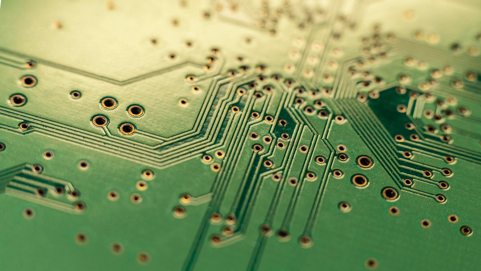
As the foundation of electronic devices, PCBs are responsible for connecting and supporting various electronic components, enabling them to work in coordination. However, during the PCB manufacturing and assembly process, there may be a seemingly minor but potentially significant risk – "burrs from outline milling."
You might wonder what kind of impact a tiny burr can have? Let me unravel this inconspicuous mystery for you.
Imagine this scenario: a renowned electronics manufacturer is developing a highly anticipated smartphone, a product that has already consumed significant resources and time, poised to create a sensation in the market.
However, during the final assembly and testing phase, they encounter a challenging issue – the battery connector of the phone fails to fit properly, resulting in an ineffective battery connection. Surprisingly, the root cause of this problem turns out to be burrs on the milled PCB.

The burr issue has not only put the company in an awkward situation of delaying product release but, more importantly, if not addressed promptly, this problem could lead to the loss of market competitiveness and even damage the brand reputation. This example vividly demonstrates the chain reaction that surface milling burrs can trigger in electronic product manufacturing.
So, what is PCB edge burr? How is it generated? This term may be unfamiliar to the general users, but when we delve into its essence, we will find that it may conceal more risks. Next, let's explore the mystery of PCB edge burr, understand its causes, and learn how to take countermeasures to ensure the stability and performance of electronic products.
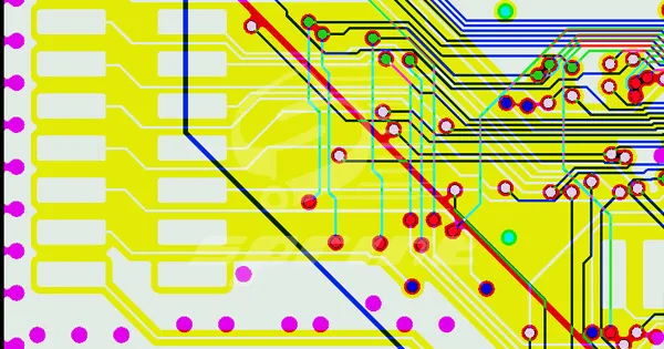
What is PCB burr on the outline milling?
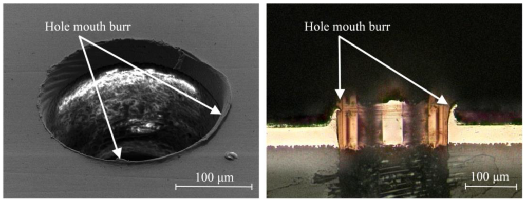
PCB burr on the outline milling refers to the tiny protrusions or sharp tips that may occur on the edge or surface of a PCB during the manufacturing process, especially during the milling operation. These burrs are typically a result of residual materials from cutting, trimming, or drilling processes, or irregularities in the manufacturing process. Burrs can consist of metal or non-metallic debris, such as copper, tin, glass fibers, etc., which may adhere to the edge or surface of the PCB.
Causes of Burrs on PCB Outline Milling
Material Selection
The hardness and properties of materials have a significant impact on the generation of burrs. Choosing harder or non-uniform materials may result in more burrs during the manufacturing process.
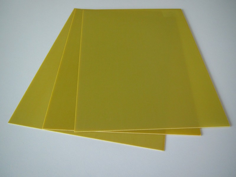
Commonly used materials in
PCB manufacturing include FR-4 (Fiberglass Reinforced Epoxy Resin) and metal substrates. Among them, FR-4, due to its higher fiberglass content, may generate more burrs during processing.
Manufacturing Process
During the processing stages such as cutting, drilling, and milling, burrs are the main issue that arises. Different processing techniques may result in varying degrees of burrs.
The sharpness of the cutting tools and processing speed in the cutting process can affect the generation of burrs. Excessively worn tools or excessively high processing speeds can easily lead to burr problems.
When drilling, the use of inappropriate tools, unreasonable cutting parameters, or excessively high drilling speeds can also cause burrs.
In the milling process, the design of the milling cutter, milling depth, feed rate, etc., will all influence the occurrence of burrs.
Equipment and Process Control
The performance and accuracy of processing equipment also influence the generation of burrs. High-precision processing equipment can minimize burr issues.
Process control is crucial for managing the generation of burrs as well. Effective process control ensures a reduction in burr formation during the manufacturing process.
PCB Design
The layout of the PCB can also affect burr issues. Unreasonable design may result in uneven stress on certain areas, leading to the generation of burrs.
To address areas prone to burrs, some design optimization measures can be taken, such as adding fillets, optimizing material distribution, etc.
Cleaning and Maintenance
In addition to the factors mentioned above, the cleanliness and maintenance of equipment also have an impact on burr generation. The accumulation of material residues or excessive wear on equipment or cutting tools may result in an increase in burrs.
Quality Control of Raw Materials
Choosing high-quality raw materials can reduce burr issues. Conducting quality control of raw material suppliers to ensure compliance with relevant standards is a crucial aspect.
Effects of PCB Edge Burrs
Difficult Connector Insertion
PCB edge burrs can cause difficulties in inserting or extracting connectors. This inconvenience may require users to apply additional force or utilize tools to connect or replace devices, thereby increasing the complexity of product usage.
Electrical Issue
Burrs may lead to short circuits or open circuits between traces, thereby affecting the overall performance of the PCB. This could result in product malfunctions, functional failures, or even damage to other components.
Signal Interference
External milling burrs on the PCB may cause signal interference, especially during high-frequency and high-speed signal transmission. This could result in decreased signal quality, leading to data transmission errors or communication interruptions.
PCB Stability Reduction
Burrs may weaken the stability and durability of PCBs, especially in vibrating or oscillating environments. Prolonged use or exposure to harsh conditions may result in loose or damaged circuit boards.
Heat Issue
Burrs may lead to ineffective heat dissipation on certain circuit boards, resulting in localized temperature rise. Elevated temperatures could potentially damage electronic components or reduce their lifespan.
Appearance and Quality
Surface milling burrs may compromise the PCB's aesthetics and overall quality, thus affecting the product's visual appeal and market competitiveness.
Safety Hazard
Burrs may cause an electrical shock risk, especially when users come into contact with exposed burrs. This represents a potential safety hazard, particularly for products requiring high levels of safety, such as household appliances and medical devices.
Increase in Production Costs
Burrs on the PCB outline will increase the complexity and defect rate during the manufacturing process. Additional steps are required to handle the burrs, leading to increased production costs and time.
Burrs on the PCB outline are a significant concern that cannot be ignored, as they can potentially impact the performance and reliability of the PCB product. In this article, we learn that burrs may lead to difficulties in connector insertion, electrical issues, and in severe cases, even cause short circuits, thus compromising the entire electronic device. Therefore, the issue of burrs during PCB manufacturing and assembly processes must be given sufficient attention.
Prevention and Handling of Burr Formation
Burr formation on the outline of the milled PCB can potentially have a significant impact on the performance of both the PCB and the overall product. Therefore, taking preventive measures and addressing the issue promptly is crucial.
Material selection
Choose high-quality PCB substrate materials to ensure a smooth surface without apparent defects. Premium materials help reduce the likelihood of burr generation.
Below are some common high-quality PCB substrate materials:
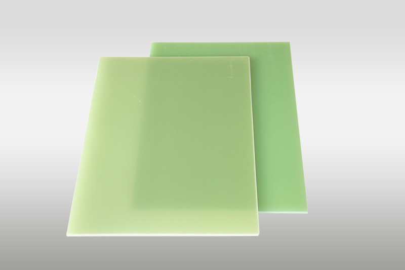
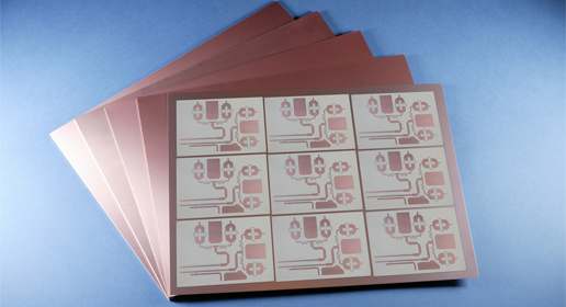
FR-4 (Fiberglass Reinforced Epoxy): FR-4 is the most common and widely used PCB substrate material. It has excellent insulation performance, mechanical strength, and thermal stability, making it suitable for most general electronic products.
 FR-4 High TG (High Glass Transition Temperature FR-4):
 This is an upgraded version of FR-4, with a higher glass transition temperature (TG), enabling it to maintain better performance in high-temperature environments. Suitable for high-temperature applications such as automotive electronics, industrial controls, etc.
 FR-4 Prepreg:
 This material undergoes partial curing during the manufacturing process, retaining a certain level of flexibility, making it suitable for
flexible PCBs that require bending or folding.
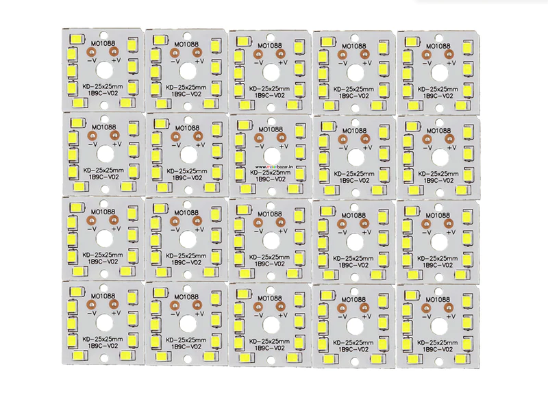
Metal Core PCB (Metal Core Printed Circuit Board): Metal Core PCBs use metal as a substrate, such as aluminum or copper. They exhibit excellent thermal conductivity and heat dissipation properties, making them suitable for high-power electronic devices, LED lights, and more.
 Ceramic Substrate:
 Ceramic substrates offer excellent high-frequency characteristics and high-temperature resistance. They are widely used in areas such as RF circuits, antennas, and microwave devices.
 PTFE (Polytetrafluoroethylene) Substrate:
 PTFE substrate exhibits excellent dielectric properties and chemical resistance, making it suitable for high-frequency and high-speed digital circuits.
Rogers Material: Rogers material is a type of special high-frequency substrate material with excellent dielectric performance and low loss, widely used in high-frequency RF circuits and microstrip applications.
 Molybdenum Substrate:
 Molybdenum substrates exhibit outstanding performance in specialized high-temperature and high-power applications, such as aerospace electronics and high-power amplifiers.
Sapphire Substrate: Sapphire substrate is a rare and advanced material used in the PCB industry, characterized by excellent optical properties and outstanding thermal conductivity. It is commonly employed in high-power lasers and optoelectronic devices.
Optimization of Processing Parameters
During the PCB manufacturing process, the rational optimization of processing parameters, such as cutting speed, tool selection, and cutting angles, can significantly reduce the probability of burr generation.
Drilling and Milling Process
Selecting appropriate drilling and milling processes to ensure precise hole diameters and surface smoothness. Using high-quality machining equipment and processes also helps to effectively reduce burrs.
Controlled Environmental Conditions
During the PCB manufacturing process, maintaining suitable environmental temperature and humidity is essential to avoid factors such as electrostatic discharge that could lead to burrs.
Edge Lithography and Polishing
Edge lithography or polishing of PCB boards helps to remove burrs and sharp edges, improving the quality of the board edges.
Deburring of PCB Outline
Inspection and Identification
During the PCB manufacturing or assembly process, inspect the surface and edges of the circuit board promptly to identify any burr issues.
Manual Deburring
For small and noticeable burrs, manual deburring can be employed using fine sandpaper, sand cloth, or a small knife to gently remove the burrs. Take care not to exert excessive force to avoid damaging the PCB.
Pneumatic Deburring Tool
For large areas or more severe burr issues, a pneumatic deburring tool, such as a pneumatic sand gun, can be used for faster and more efficient processing.
Chemical Treatment
In certain cases, chemical treatment methods can be employed, utilizing chemical agents or solutions to dissolve or soften burrs, which can then be removed by jetting or cleaning.
Edging Technology
Some
PCB manufacturers employ edging technology, utilizing special materials or coatings to encase the edges of the board, preventing the generation of burrs.
Grinding and Polishing
For highly severe burr issues, mechanical grinding or chemical mechanical polishing methods can be employed to achieve a smooth and flat surface on the PCB.
It is important to note that when dealing with burrs, caution must be exercised to avoid damaging the PCB. For PCBs produced in large quantities, it is advisable to take preventive measures during the manufacturing process to reduce burr generation. This way, subsequent handling can be carried out more efficiently.
Addressing the issue of burrs in PCB milling is a crucial aspect of the PCB manufacturing and assembly process, as it directly impacts the performance and reliability of electronic products. By preventing and promptly handling burrs, PCB quality can be improved, ensuring products remain competitive in the market and meet the needs and expectations of users.
Trust
SprintPCB to let your creativity shine on the world stage. Our professional team will go above and beyond to meet your PCB needs and ensure your design stands out in terms of quality and performance. Whether you are an electronics manufacturer, engineer, or maker, we tailor the best solutions for you. Visit our official website to embark on a new chapter of your design journey!