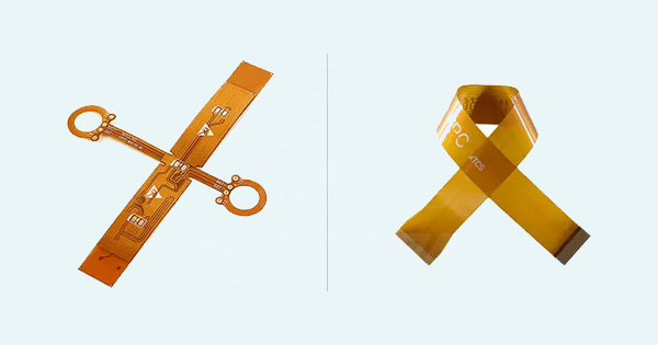
Flexible PCBs (Flex PCBs) are essential in industries such as aerospace, consumer electronics, and medical devices due to their ability to bend, fold, and conform to complex shapes. This article offers a detailed overview of the manufacturing processes involved in creating multi-layer flexible PCBs, emphasizing their advantages and the materials used.
The foundation of a high-quality flexible PCB lies in the materials chosen. Common materials include polyimide (PI) and polyester (PET) as the substrate, coupled with conductive copper foils. These materials are selected based on their flexibility, heat resistance, and electrical conductivity, making them suitable for various high-performance applications.
Key Materials:Copper Foil: Available in different thicknesses (1oz, 1/2oz, 1/3oz), used for creating conductive paths.Substrate Films: Typically 1 mil or 1/2 mil thick, providing the flexible base.Adhesives: Thickness varies based on customer requirements, used for bonding copper to the substrate.
Before diving into manufacturing, the design phase is critical. A well-thought-out design ensures that the Flex PCB is not only functional but also manufacturable. Key considerations include:
Design for Manufacturability (DFM): Ensures the design can be efficiently and reliably manufactured.Layout and Routing: Proper signal integrity and electromagnetic compatibility (EMC) are crucial.Multilayer and Rigid-Flex Designs: These require careful planning to balance flexibility with mechanical strength.
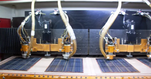
The process begins with the preparation of materials. Key materials include flexible substrates (such as polyimide), copper foils, adhesives, and coverlays. These materials are typically supplied in rolls and must be carefully slit or cut to the required sizes using a slitting machine.
Drilling is the next step, where vias (plated through holes) are created to allow electrical connections between layers. Given the flexible nature of the material, special attention is needed to prevent burrs and delamination during drilling. Advanced mechanical drilling or laser drilling methods are employed to create precise holes that align with the design specifications.
After drilling, the vias need to be metallized to create a conductive path between the layers. This is done through a series of steps:Desmearing: The inner walls of the drilled holes are cleaned to remove any debris or resin smear, ensuring good adhesion for the plating process.Electroless Copper Plating: A thin layer of copper is deposited onto the hole walls through a chemical process, ensuring uniform coverage.Electrolytic Copper Plating: A thicker copper layer is applied through electroplating to reinforce the initial deposit, providing robust conductivity between layers.
The multi-layer FPC now undergoes the image transfer process:
Lamination of Dry Film: A photosensitive dry film is laminated onto the copper surfaces. This film will help define the circuit patterns.Exposure: The laminated board is exposed to UV light through a photomask that outlines the desired circuit patterns. The UV light hardens the exposed areas of the dry film.Development: The unhardened areas of the film are then washed away, exposing the underlying copper that needs to be etched.Etching: The exposed copper areas are etched away using a chemical solution, leaving behind the circuit patterns defined by the hardened dry film.Stripping: The remaining dry film is stripped away, revealing the final copper traces that form the circuit.
Multi-layer FPCs require precise lamination of several layers to ensure that the conductive traces align correctly. This process involves:Layer Stack-Up: Individual layers, including conductive and insulating layers, are aligned and stacked in the correct order.Lamination: The stack is then subjected to heat and pressure in a vacuum environment, which bonds the layers together. The adhesive materials melt and cure, forming a strong, unified structure.
To protect the delicate circuitry, a coverlay (or cover film) is applied. This step involves:Coverlay Cutting and Preparation: The coverlay film, which is usually made from polyimide, is cut to the required shape with openings for soldering pads.Lamination: The coverlay is laminated onto the circuit, using heat and pressure to bond it securely. This protects the circuit from environmental factors and physical damage while maintaining flexibility.
To ensure good solderability and protect the copper pads from oxidation, a surface finish is applied. Common surface treatments include:ENIG (Electroless Nickel Immersion Gold): A thin layer of nickel is deposited, followed by a layer of gold. This finish provides excellent corrosion resistance and ensures reliable soldering.
The FPC must undergo electrical testing to verify the continuity and insulation between traces. This step is crucial to identify any short circuits, open circuits, or other defects that could compromise the PCB's performance.
After passing the electrical tests, the FPC is cut to its final shape and size using laser cutting or mechanical punching. This step ensures the board fits perfectly into its intended application.
The final inspection ensures that the multi-layer FPC meets all the required specifications and quality standards. This includes visual inspection, dimensional checks, and more detailed testing as needed.
The finished FPCs are carefully packaged to prevent any damage during transportation. They are then shipped to the customer for assembly into the final product.
This detailed process illustrates the complexity and precision required in manufacturing multi-layer flexible PCBs. Each step is critical to ensuring that the final product meets the high standards required for modern electronic devices.
Flexible PCBs offer several advantages that make them superior to rigid PCBs in certain applications:
High Flexibility: Flex PCBs can be bent, folded, or twisted, allowing for complex, three-dimensional configurations.Space and Weight Saving: They contribute to the miniaturization of devices by reducing space and weight.High Reliability: Suitable for high-density applications where reliability is crucial, such as in aerospace equipment.Heat Dissipation: Flex PCBs exhibit excellent thermal management, which is crucial in high-performance electronics.Cost-Effectiveness: Despite their complex manufacturing process, Flex PCBs can reduce overall system costs by integrating multiple functions.
Flex PCBs are categorized based on how the copper foil is bonded to the substrate:
Adhesive-Based Flex PCBs: Copper foil is bonded using adhesive. This is the most common type.Adhesive-Free Flex PCBs: Copper is bonded directly to the substrate using heat and pressure, offering better flexibility and stronger bonds but at a higher cost.
Copper Foil: Can be electro-deposited or rolled, providing the conductive layer.Substrate: A flexible polymer material that supports the copper traces.Adhesives: Used to bond copper to the substrate, depending on the application.Coverlay: An insulating layer that protects the circuits from damage and environmental exposure.Reinforcement Layers: Like PI films, these are used to add mechanical strength for specific areas, such as where components are mounted.
Producing Flex PCBs involves several challenges, particularly in handling the delicate materials. Solutions include:
High-Precision Drilling: To prevent defects like burring, using advanced drilling techniques is essential.Efficient Material Handling: To avoid contamination and defects, materials are handled in clean environments with precision machinery.Surface Treatment: Advanced surface treatments like ENIG are used to ensure durability and reliability.
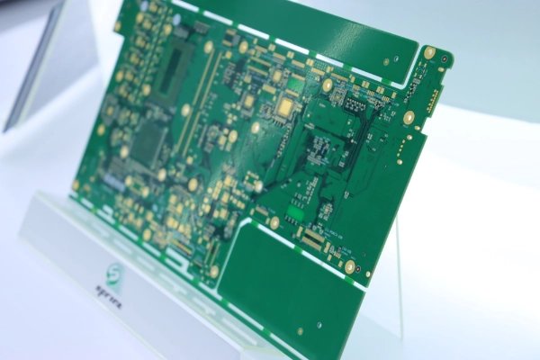
The manufacturing of flexible PCBs is a complex and meticulous process that demands precise control and high-quality materials. By mastering each stage—from material selection to final inspection—manufacturers can produce Flex PCBs that meet the stringent demands of modern electronics. SprintPCB excels in this process, utilizing advanced technology and rigorous quality standards to deliver flexible PCBs that are essential for creating smaller, more powerful, and reliable electronic devices.

Customer support