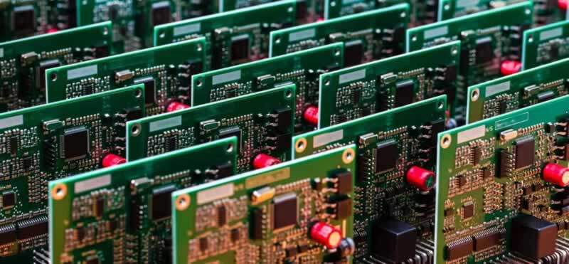
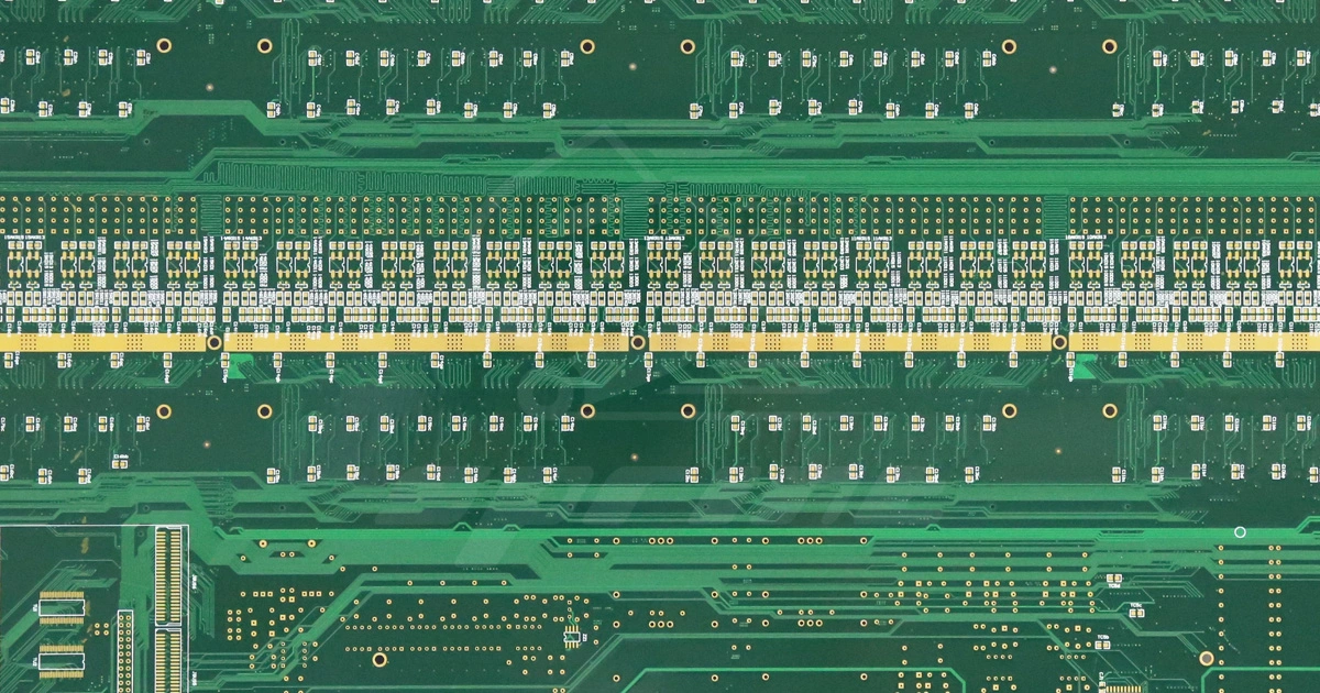
In the electronic manufacturing industry, Printed Circuit Board (PCB) assembly is a critical process. High-quality PCB assembly not only ensures the reliability and performance of the product but also enhances production efficiency and reduces costs. However, achieving excellence in PCB assembly is not an easy task. This article will reveal 9 secrets to help you achieve flawless production in the PCB assembly process.
Secret 1: The Importance of Design Optimization and DFM (Design for Manufacturing)
In PCB assembly, design optimization and the principles of Design for Manufacturing (DFM) play a crucial role. By closely collaborating with the manufacturing team, you can consider manufacturing feasibility during the design stage, optimize layouts, reduce assembly complexities, and ensure efficient production processes.
Secret 2: Choosing the Right Component Packages and Suppliers
Choosing the appropriate component packages for your application requirements is crucial. Different package types have different characteristics and suitability. Furthermore, selecting reliable suppliers is essential for obtaining high-quality components and ensuring the stability and reliability of the supply chain.
Component packaging refers to the external encapsulation form of electronic components. There are several common types of component packages available, including:
Dual In-line Package (DIP): A package with two rows of pins, commonly used for early integrated circuits and plug-in components.
Small Outline Integrated Circuit (SOIC): A common surface-mount package suitable for applications with high-density wiring.
Quad Flat Package (QFP): A package with multiple pins, widely used in medium to high-density integrated circuits.
Ball Grid Array (BGA): A package with a set of small ball-shaped solder balls as pins, suitable for high-density and high-performance integrated circuits.
Land Grid Array (LGA): Like BGA but uses metal pads instead of solder balls as pin connections.
Chip Scale Package (CSP): A package with dimensions close to the size of the chip itself, commonly used in compact electronic devices.
Thin Small Outline Package (TSOP): A package suitable for memory chips and other applications.
Plastic Leaded Chip Carrier (PLCC): A square-shaped package with leads for pins.
Through-Hole Technology (THT): A technology that connects components by inserting the pins into holes in the printed circuit board.
These are just a few common types of component packages, and there are many other packaging options available. Each package type has its specific advantages and application range. When selecting component packages, it is important to consider factors such as design requirements, PCB layout, and manufacturing feasibility.
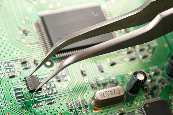
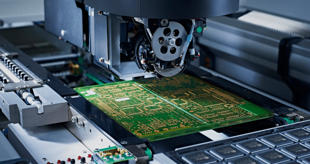
Secret 3: Accurate Component Placement and Alignment
In the process of PCB assembly, precise component placement and alignment are crucial steps. Ensuring correct component placement and precise alignment can help avoid soldering issues such as short circuits or cold solder joints.
Soldering issues can lead to various quality and performance issues during PCB assembly. Here are some common soldering problems and their potential consequences:
Cold solder joint refers to an insufficiently bonded solder connection where the solder joint is not fully melted and wetted. Its hazards include:
Increased resistance: Cold solder joints can increase the electrical resistance, potentially leading to poor signal transmission or compromised circuit functionality.
Reduced mechanical strength: Cold solder joints have inadequate strength, making them prone to fracture under vibration or stress.
A short circuit refers to the unintended electrical connection between two or more solder points that should not be connected. Its hazards include:
System failure: A short circuit can lead to abnormal circuit functionality or the inability of the entire system to operate properly.
Component damage: The short circuit current may exceed the rated value of the components, causing damage or destruction to the components.
Overheating refers to the condition in which the temperature during the soldering process is too high or the soldering time is too long, resulting in excessive heat on the components or solder pads. Its hazards include:
Component damage: Overheating can cause damage to the internal structure of components, resulting in reduced performance or complete destruction.
Solder pad damage: Overheating can cause the solder pad material to melt or lose adhesion, affecting the reliability of soldering connections.
Poor Solder Fillet, characterized by uneven or excessive/insufficient solder distribution and irregular solder joint formation, can have the following implications:
Unreliable electrical connection: Poor Solder Fillet can result in an unstable electrical connection between solder joints, thereby impacting the overall circuit's transmission performance.
Reduced mechanical strength: The irregular shape of poor solder fillets can compromise the mechanical strength of the solder joint, making it more susceptible to fracture under stress or vibration.
The extent of the hazards posed by these issues depends on their location, quantity, and severity. To avoid these problems, proper soldering techniques and process specifications should be followed, ensuring appropriate temperature, time, and use of soldering materials, along with quality control and inspection measures.
Secret 4: Control Soldering Temperature and Time
Soldering temperature and time are crucial for achieving good soldering quality. Using excessively high temperatures or prolonged soldering times can damage components or result in poor solder joints. It is essential to control the appropriate temperature and time to ensure reliable solder connections.
The standards for soldering temperature and time depend on the specific soldering process and the soldering materials used. Different soldering applications and component packages may have different temperature and time requirements.
Surface Mount Technology (SMT) Soldering
Soldering Temperature Range: Typically, between 220°C to 250°C, depending on the solder material and component package.
Soldering Time: Typically, between 10 seconds to 30 seconds.
Double-Sided Through-Hole Soldering
Soldering Temperature Range: Typically, between 250°C to 300°C, depending on the solder material and component package.
Soldering Time: Typically, between 3 seconds to 5 seconds.
Secret 5: Use high-quality solder and flux
Choosing high-quality solder and flux is crucial for achieving flawless soldering. Premium solder and flux provide excellent wetting properties and reliable solder connections, reducing the risk of soldering defects.
There are many reputable brands of solder and flux available in the market. Here are some commonly used brands and types.
Kester is a well-known manufacturer of solder and flux, offering a variety of products such as lead-free solder, no-clean flux, and organic acid flux.
Alpha Assembly Solutions is a globally leading supplier of soldering materials, providing a wide range of solder and flux products, including lead-free solder, tin-lead alloy solder, and bonding agents.
Multicore, a brand under Henkel, offers various types of solder and flux, including lead-free solder, tin-lead alloy solder, repair solder, and flux modifiers.
Indium Corporation specializes in high-performance soldering materials, offering a variety of solder and flux types such as lead-free solder, micro-solder, and high-temperature solder.
Aim Solder is a globally leading supplier of soldering materials, providing multiple types of solder and flux, including lead-free solder, tin-lead alloy solder, and specialty alloy solder.
These brands offer solder and flux that have a good reputation for quality, performance, and reliability. Depending on your specific application needs and requirements, you can choose a brand and type that is suitable for your project. Before making a selection, it is advisable to consult with the supplier or manufacturer to obtain more specific advice and recommendations.
Secret 6: Proper ESD Protection and Electrostatic Control
Electrostatic discharge (ESD) can potentially damage the PCB assembly process. By correctly using ESD protective equipment and controlling static electricity, you can safeguard the PCB and sensitive components during the assembly process, ensuring flawless production.
Correct ESD protection and electrostatic control include the following practices:
Wearing appropriate antistatic clothing or using antistatic gloves to prevent the accumulation and discharge of static charges.
Using antistatic mats or workbenches in the workspace to redirect static charges to the ground, avoiding static discharges.
Storing and transporting sensitive components in antistatic containers or packaging materials to protect them from electrostatic damage.
Using suitable ESD protection tools and equipment, such as static eliminators and ESD mats, to control the release and conduction of static electricity.
Avoiding operations in dry environments, as dry air increases the risk of static charge accumulation and discharge.
Establishing good workflow and operating procedures, including handling and operating steps for electrostatic-sensitive components, to minimize the impact of static electricity.
Regularly testing and inspecting the work area for ESD compliance to ensure the effectiveness of antistatic measures and compliance with standards.
Training employees on the importance of electrostatic control and proper handling methods to enhance their awareness and skills.
By implementing these simple measures, the impact of static electricity can be reduced, protecting sensitive PCB assembly processes and components, and ensuring flawless production.
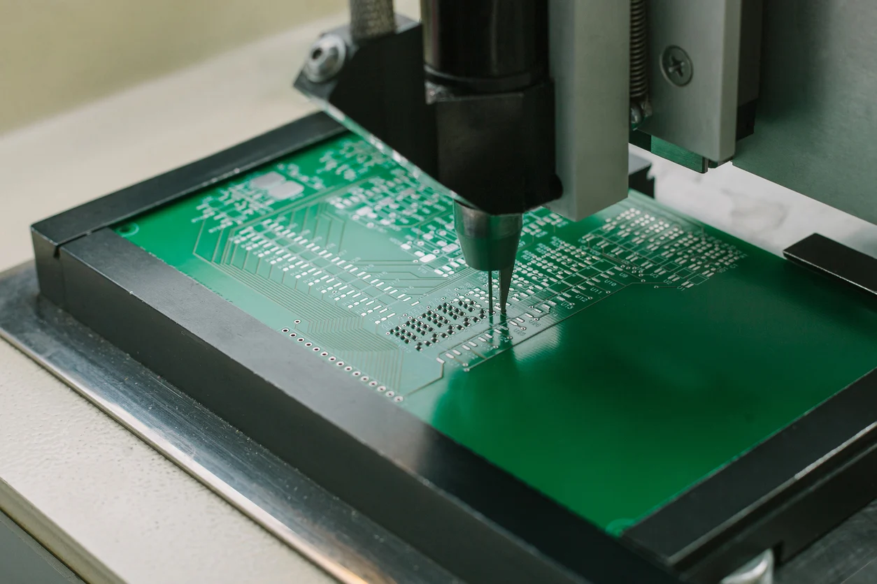
Secret 7: Implement Rigorous Quality Control and Inspection Processes
Rigorous quality control and inspection processes are the foundation for achieving excellence in PCB assembly. By utilizing various quality control tools and inspection methods, you can promptly identify and rectify any potential quality issues, ensuring that your products meet standards and specifications.
During the quality control and inspection process of PCB assembly, the following are some commonly used tools and methods.
Visual Inspection: Use naked eye to examine the appearance of PCB assembly to ensure there are no obvious soldering defects, component misplacements, or damages.
X-ray Inspection: Utilize X-ray radiation to examine the internal quality of soldering connections on the PCB. This method is particularly useful for detecting issues that may not be visible through visual inspection, such as cold solder joints, excessive or insufficient soldering, etc.
Thermal Profiling: Employ thermal profiling instruments to monitor the temperature distribution and time curve during the soldering process, ensuring that the soldering temperature and time are within appropriate ranges.
PCB Testing: This includes electrical testing and continuity testing to ensure the circuit connections on the printed circuit board are accurate and error-free.
Soldering Quality Inspection: Use soldering quality inspection equipment such as solder peel strength testers, solder joint reliability testers, etc., to evaluate the reliability and strength of soldering connections.
AOI (Automated Optical Inspection): Utilize automated optical inspection devices to perform high-speed scanning and image analysis of the PCB to detect soldering defects, component misplacements, or damages.
ICT (In-Circuit Testing): Employ in-circuit testing equipment to conduct functional and electrical tests on the PCB to verify the correct operation and performance of the circuit.
ESD Testing: Use ESD testing instruments to detect and control electrostatic discharge to prevent damage to sensitive components and circuits.
Reliability Testing: This includes environmental testing (such as temperature cycling, humidity testing) and reliability lifespan testing to evaluate the reliability and durability of PCB assembly under various conditions.
Secret 8: Continuous Learning and Team Collaboration
Continuous learning and team collaboration are crucial for achieving excellence in PCB assembly. With the constant development of PCB assembly technology, staying updated with new techniques, training team members, and exchanging experiences with manufacturing experts and peers allows you to continually enhance your PCB assembly skills.
Secret 9: Tracking and Analyzing Data for Process Improvement
Tracking and analyzing data are key to improving the PCB assembly production process. By collecting and analyzing key data metrics, you can identify potential bottlenecks and improvement opportunities, and act appropriately to enhance production efficiency and quality.
Achieving excellent PCB assembly requires considering multiple factors holistically, from design optimization to soldering techniques, and from quality control to teamwork. By following these 9 secrets, you can enhance the quality, efficiency, and reliability of PCB assembly, moving closer to the goal of flawless production.
Elevate Your PCB Manufacturing with SprintPCBSprintPCB stands as a prominent high-tech enterprise, delivering exceptional PCB manufacturing services to clients across the globe. With our extensive industry experience and competitive pricing, you can direct your focus towards the most crucial aspects of your organization. Contact us today to discover how we can collaborate and help you achieve your goals.