HDI PCB Fabrication is a transformative technology enabling the creation of compact, efficient, and high-performance electronic devices despite its complexity and cost.
High-density interconnect (HDI) PCB fabrication is a cornerstone technology in the electronics manufacturing industry, enabling the development of more compact, efficient, and high-performance devices. As electronic devices continue to evolve towards greater functionality packed into smaller form factors, understanding the basics of HDI PCB fabrication becomes crucial for designers aiming to leverage these advancements for efficient design.
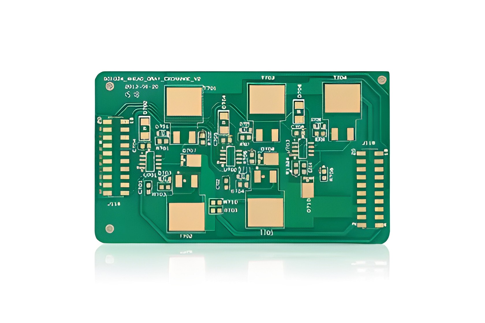
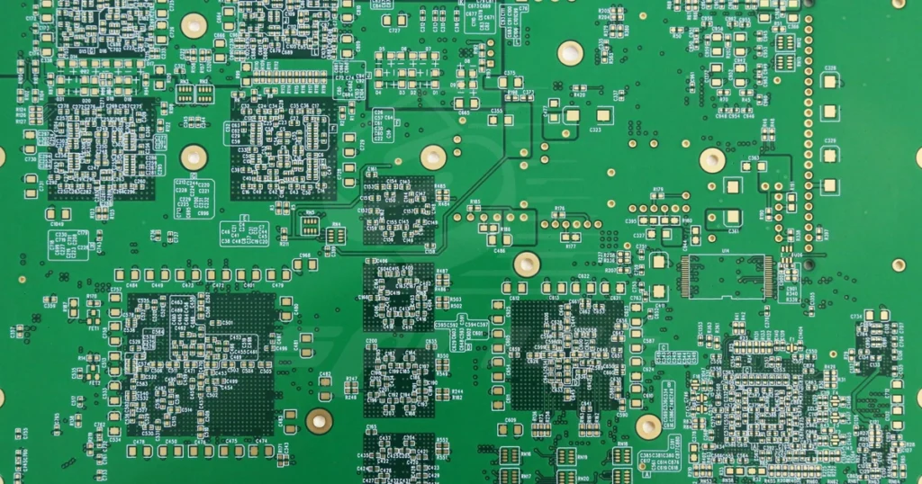
HDI PCB fabrication refers to the process of creating printed circuit boards (PCBs) that feature a higher wiring density per unit area compared to conventional PCBs. This is achieved through the use of finer lines, smaller vias (holes), and tighter spaces and annular rings, allowing for more components to be placed on both sides of the raw PCB material. The essence of HDI technology lies in its ability to enhance electrical performance while simultaneously reducing size and weight.
Microvias: Small vias with diameters typically less than 0.006 inches (150 micrometers), used to connect different layers of a PCB with less space.
Fine Lines and Spaces: Narrower circuitry lines allow for more circuits per unit area.
Increased Density: Allows for more components to be mounted, facilitating greater functionality in a smaller space.
Improved Electrical Performance: Reduces signal loss and cross-talk, crucial for high-speed designs.
By reducing the distance between components, HDI PCBs can significantly improve signal integrity, making them ideal for high-speed and high-frequency applications. This is particularly important in the era of gigahertz signal processing where every millimeter counts.
HDI technology plays a pivotal role in the miniaturization of electronic devices. With the ability to place more components on a smaller board, designers can create compact devices without compromising on performance.
While the initial cost of HDI PCB fabrication might be higher than traditional methods, the overall cost benefits become apparent in the long run. Reduced material usage, lower energy consumption, and the ability to integrate multiple functions into a single board can lead to significant cost savings.
Despite its numerous advantages, HDI PCB fabrication presents certain challenges that need to be addressed:
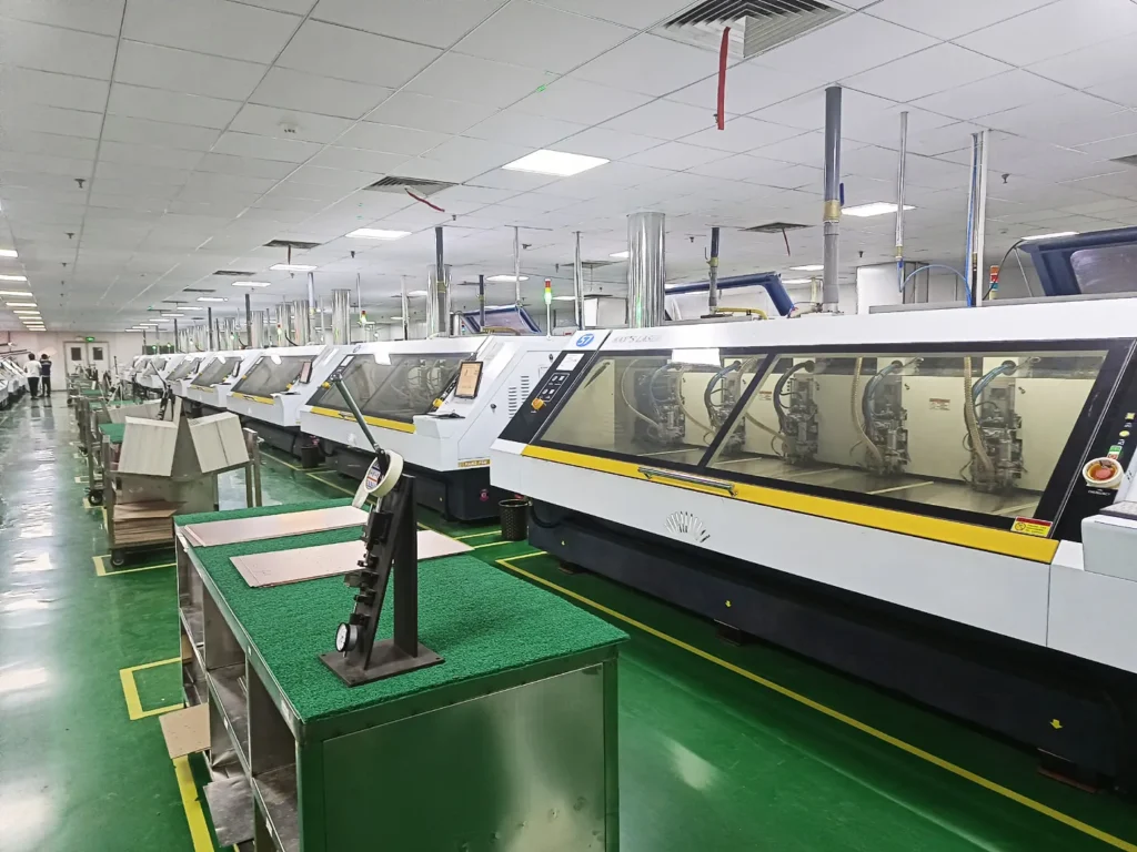
Complex Manufacturing Process: The fabrication of HDI PCBs involves sophisticated processes that require precise control, making them more complex than conventional PCB manufacturing.
Design Constraints: Designers must consider the limitations and requirements of HDI technology, such as via placement and routing strategies, to fully utilize its potential.
Higher Initial Costs: The advanced equipment and processes required for HDI PCB fabrication can lead to higher upfront costs compared to standard PCB production.
HDI PCB fabrication is a transformative technology that enables the development of smaller, faster, and more efficient electronic devices. By understanding the basics of HDI PCB fabrication, designers can harness its full potential to create innovative products that meet the demands of today's technology-driven world. Despite the challenges associated with its complexity and cost, the benefits of miniaturization, enhanced performance, and cost efficiency make HDI PCB an indispensable tool in the electronics design arsenal.

Customer support