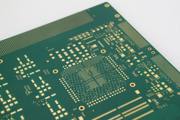
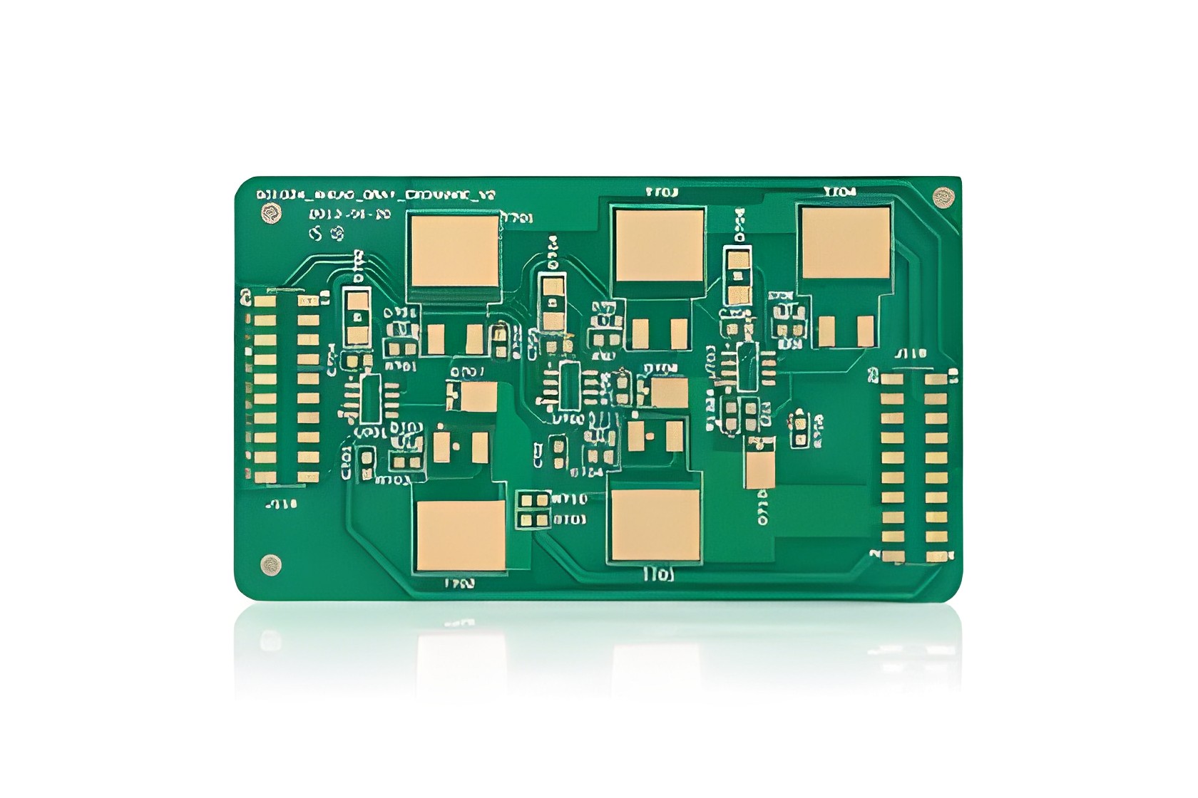
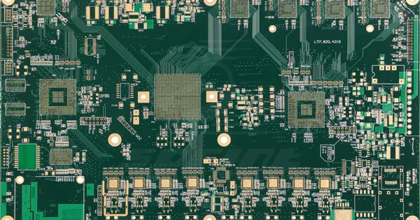
In high-frequency PCB design, interference issues become increasingly complex as frequencies rise and circuits become smaller and more cost-effective. The main interference factors include power noise, transmission line interference, coupling, and electromagnetic interference (EMI). Here’s a detailed explanation and solutions:
1. Power Noise
In
high-frequency PCB design, power noise significantly affects high-frequency signals. Therefore, low-noise power is essential, along with clean ground and power lines. Power has inherent impedance, and noise can overlay on the power supply. To minimize power impedance, dedicated power and ground layers are preferred. Power layers are generally better than bus designs, minimizing signal loops and reducing noise.
Methods to Eliminate Power Noise:
- Via Management: Avoid large openings in power layers that disrupt signal loops. Large openings can force signals to detour, increasing loop area and noise.
- Sufficient Ground Lines: Each signal needs a dedicated return path, with parallel signal and return paths, minimizing loop area.
- Separate Analog and Digital Power: High-frequency devices are sensitive to digital noise, so separate them and merge at the power entry point, with loops placed for crossing signals.
- Avoid Overlapping Power Layers: Prevent noise coupling through parasitic capacitance.
- Isolate Sensitive Components: For example, PLLs.
- Place Power Lines: Reduce noise by placing power lines adjacent to signal lines.
2. Transmission Lines
In high-frequency PCB design, transmission lines face reflection issues, which degrade signal quality and increase system noise. The primary solution is impedance matching, avoiding discontinuities in transmission line impedance.
Methods to Eliminate Transmission Line Interference:
- Avoid Impedance Discontinuities: Use 45° angles or curves instead of right angles, and minimize via usage, as each via is a point of impedance discontinuity.
- Avoid Stub Lines: Short stub lines can be terminated; long stub lines should be avoided as they cause significant reflection.
3. Coupling
In high-frequency PCB design, common coupling channels include common impedance coupling, common-mode coupling, differential-mode coupling, and crosstalk.
Methods to Eliminate Crosstalk:
- Proper Termination: Terminate sensitive signal lines to reduce interference.
- Increase Distance Between Signal Lines: Use ground layer management and reduce lead inductance.
- Insert Ground Lines: Between adjacent signal lines, with ground lines connected to the ground plane every 1/4 wavelength.
- Minimize Loop Areas: Reduce loop size where possible.
- Avoid Shared Signal Loops: Ensure each signal has a unique return path.
- Focus on Signal Integrity: Use termination techniques during soldering and copper foil shielding for microstrip lengths.
4. Electromagnetic Interference (EMI)
In high-frequency PCB design, as speeds increase, EMI issues become more significant, especially for high-speed devices.
Methods to Eliminate Electromagnetic Interference:
- Reduce Loops: Minimize the number and size of loops, avoid artificial loops, and use power planes.
- Filtering: Use decoupling capacitors, EMI filters, and magnetic components on power and signal lines.
- Shielding: Implement shielding measures, such as shield cans or layers.
- Lower High-Frequency Device Speed: Choose lower-speed devices to reduce EMI.
- Increase PCB Dielectric Constant and Thickness: Reduce radiation from high-frequency parts and prevent electromagnetic leakage.
Summary principles for high-frequency PCB design:
- Unified and Stable Power and Ground: Ensure low-impedance, clean power, and ground lines.
- Careful Routing and Termination: Eliminate reflections and reduce crosstalk.
- Noise Suppression: Use filtering, shielding, and optimized design to meet EMC requirements.